10.1. OP/AMPS PRINCIPLE
10.1.1. Op/amps Without Feedback
10.1.2. Op/amps With Feedback
10.2. NON-CONTACT SENSORS
10.2.1. Temperature Sensors
10.2.2. Humidity Sensors
10.2.3. Ultrasonic Sensors
10.2.4. Photo Sensors
10.2.5. Proximity Sensors
10.2.6. Electromagnetic Sensors
10.3. CONTACT SENSORS
10.3.1 Force/Pressure Sensors
10.3.2. Thickness/ Displacement Sensors
PROBLEMS
REFERENCES
PART 10- SENSORS THEORIES AND APPLICATIONS
All the basic instruments discussed in chapter PART 7 are used in industrial measurement. In addition, industrial instruments monitor and measure outputs of sensors for process control. Unfortunately, the output quantities such as volt or resistance of sensors are so small that make it difficult to use them directly without amplification to control the process. Thus, signal conditioning or modification is needed to adjust the output level to a measurable value. Operational amplifiers are universally used to achieve this objective. In this part, basic principle of op/amps will be discussed first, followed by theories of several sensors. Finally, to understand the overall picture, several practical examples using op/amps will be described. Problems and additional references are included at the end of this chapter for missing parts.
10.1. OP/AMPS PRINCIPLE
At this time, reader is requested to refer to the circuit diagram of a typical op/amp such as IC 741 shown on figure 9-2, PART 9. Special attention must be given to the input difference amplifiers, Q1 and Q2. This amplifier controls the entire operation of IC 741. The electronic symbol of overall amplifier, repeated figure 10-1.
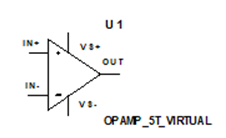
Fig.10-1. Electronic symbol of a general op/amp
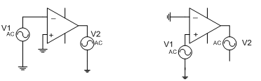
10.1.1. Op/amp Without Feedback: Op/amp shown in figure 10.1 has no feedback, i.e. output is isolated from the input, this is called open loop difference amplifier. Such amplifier can be used in two different modes depending on the inputs. One mod is using it with one input, the other input being grounded as shown in figure 10-2 (a, b). Figure 10-2(a) is referred to as inverting amplifier since the output (v2) is inverted with respect to the input terminal. Figure 10-2(b) is referred to as non-inversing amplifier with the similar reasoning.
(a) (b)
Fig.10-2 Two different modes of op/amps (a) Inverting amplifier
(b) Non-inverting amplifier
The other, the most practical mode is to use op/amp with two different inputs shown in figure10-3.
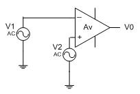
Fig.10-3 General use of op/amp with two inputs
The output can be written as:
Vo = Av (V2 – V1) (10-1)
This equation can be used for other modes mentioned earlier with appropriate terminal grounded. It is to be emphasized that the voltage gain Av of such amplifier, i.e. op/amp without feedback is extremely large, in the order of 10,000-106 and it is this feature, which makes it attractive for NMR or EKG applications. However, it cannot be used in electronics if the integrity of signal shape has to be reserved since higher gain will always result in distortion. However, it can be used for comparison purposes as shown in figure 10-4.
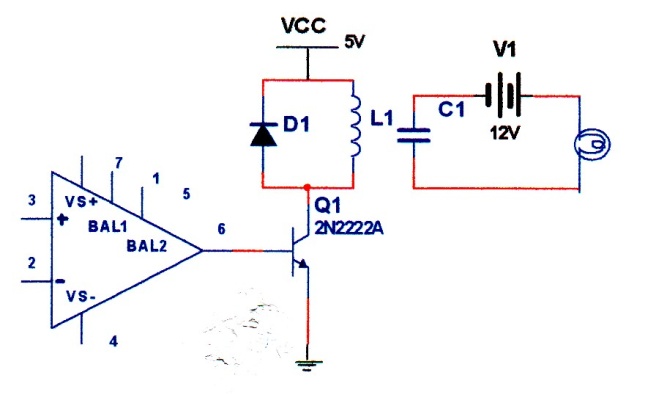
Fig.10-4. Op/amp without feedback used as a comparator
In this application, two inputs are applied to terminals 2 and 3. A constant reference voltage is applied to terminal 2 and an unknown voltage such as the output of a thermocouple can be applied to terminal 3. If V3 exceeds the reference voltage, Q1 will be turned on and relay will be energized, its contact will be closed, and finally warning light will come on. The operation of this circuit can be described simply by following relations:
If V3 < V2 Vo = – (light off) (10-2)
If V3 > V2 Vo = + (light on) (10-3)
Note that sign of Vo depends on which input is larger. If V3 is larger than V2, then transistor, being NPN, will turn on, energizing relay. Also, note that in this configuration transistor acts as a switch not as an amplifier. The circuit is used only as a comparator not for measurement. It does not measure the value of the input, as soon as its input exceeds reference voltage, warning light will come one. For consistent operation, the circuit requires constant reference voltage. Constant voltage can be derived from a Zener diode as shown in figure 10-5, (see problem section).
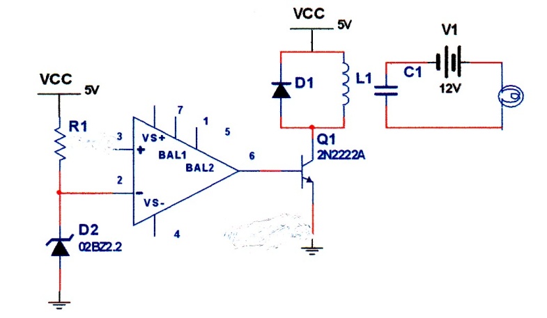
Fig. 10-5 A comparator with a constant reference voltage using a Zener diode
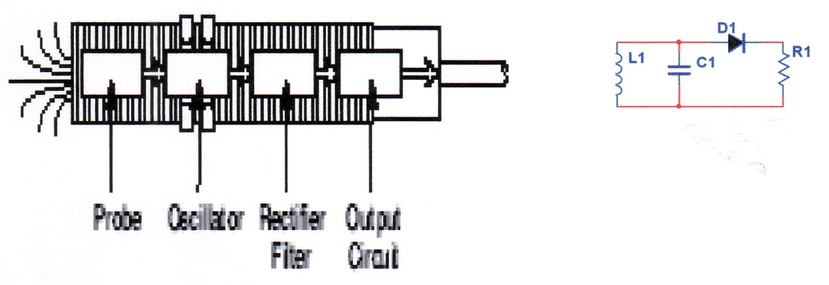
This circuit can be used only in On/off process control. It has certain limitation. It is very sensitive, it can turn on or off under small vibration or noise. Thus, a more reliable switching circuit is needed. This requires op/amps with feedback, the topic of next section. The diode D1 is used to discharge the inductor current when transistor goes off. Without this diode, a large impulse current resulting from the inductor turning off may destroy the transistor.
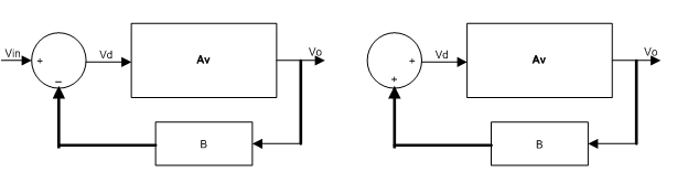
10.1.2. Op/amps With Feedback: A portion of output fed back to the input to form a closed loop circuit is called feedback. Two types are common, positive feedback and negative feedback shown in figure 10-6.
 (a) (b)
Fig. 10-6-Two types of feedback system (a) negative feedback (b) positive feedback
The closed loop gain for both systems is given by (see problem section):
Note that + is used for negative feedback and – is used for positive feedback. Positive feedback is used to generate a desired waveform such as sine wave. This subject is treated in Part 6, but negative feedback is used to control the process and will be covered in detail in the following section. Before proceeding with negative feedback, we should emphasize that feedback has several effects on amplifier operation. It affects amplifier gain, frequency response, input/output impedances, depending whether feedback is positive or negative. Interested readers are encouraged to review feedback concepts in most electronic textbooks.
Two types of op/amps are commonly used for industrial control with negative feedback, inverting and non-inverting amplifiers shown in figure 10-7. These are the same as given in figure 10-2 except for the feedback circuits.
(a) (b)
Fig.10-7 Two types of op/amps with negative feedback
(a) Inverting amplifier (b) Non-inverting amplifier
Above equations are derived under the following condition:
and
These equations describe ideal op/amp characteristics. They are one equation expressed in different forms, one applies the other. In dealing with op/amps, these equations must be kept in mind. Note that they refer to the internal structure of the op/amp not to the external circuitry. For example, to arrive at equations (10-5) we assume that potential at terminal 2 and 3 are almost the same, thus no input current flow in to the op/amp, therefore, the input current must flow in to external resistor R1 or R3/R4. If we apply this principle, equation (10-5), and all other complicated equations of op/amps can be obtained, (See problem section). The non-inverting amplifier shown in figure 10-7(b) has one important property. If we set R3= 0, Vo becomes:
R3 = 0, Vo = V2 ≈ Vin (10-7)
Such op/amp has a voltage gain of one. It is called a buffer. It can be used for impedance matching since its input impedance as described by equation (10-6) is infinite and its output impedance Ro is zero.
10.1.2.1. Two-Level Comparator: As mentioned earlier on/off comparators are very sensitive and can switch their states under small fluctuation or plant noise. Two level comparator can provide needed noise margin but at the expense of hysteresis. However, these two parameters are in conflict, increasing noise margin also increase hysteresis. Thus it becomes the responsibility of circuit designer to obtain an optimum values with greater noise margin but smaller hysteresis. Following method is suggested to resolve this problem. A typical two level comparator is shown in figure 10-8; it is usually referred to as Schmitt Trigger.
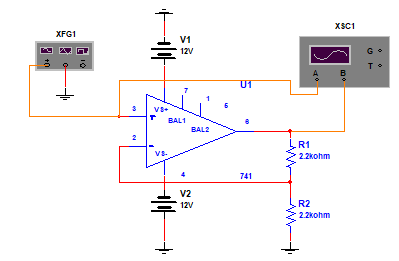
Fig. 10-8 A two level comparator- the Schmitt Trigger
Figure 10-9, shows input-output waveforms. As seen from the figure, input is a sine wave of 15V peak, with 1ms duration. Output is a square wave with 16V and –7V peak. Note that regardless of the input waveform, the output waveform will always be a plus/minus rectangular wave if the input voltage at terminal 3 exceeds the reference voltages.
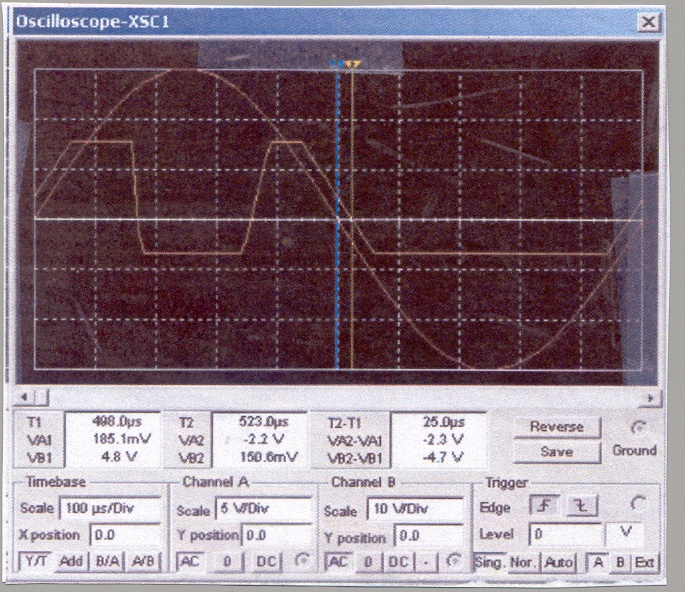
Fig. 10-9 Input-output wave forms of the Schmitt Trigger shown in figure 10-8
Note that two level comparator such as above requires two separate reference voltages, high and low; applied to terminal 2. Strangely enough, these two voltages are derived from the output using negative feedback. These are calculated as following:
Where +/- refer to high/low output conditions. Returning now, to noise margin and hysteresis effects. As mentioned above, two level comparator could provide extra safety noise margin with the expense of hysteresis. It is seen from figure 10-9 that output does not drop to zero when input attains zero. Output becomes zero after a delay. This is the hysteresis effect of Schmitt trigger. Although in industrial application this delay may be, tolerable but in digital switching systems, it can be a limiting factor. A desirable switching system should have small hysteresis time with maximum noise margin, but as mentioned above, these two parameters are in conflict. Following method is suggested to optimize the performance. The normalized noise margin is given by:
V+ and V– refer to upper and lower voltage levels. The normalized hysteresis time is calculated to be (see problem section).
A plot of n and th are shown in figure 10-.10. Since n is an increasing function but th is a decreasing function of R2, the intersection of these two curves establishes the proper choice for R1 and R2.
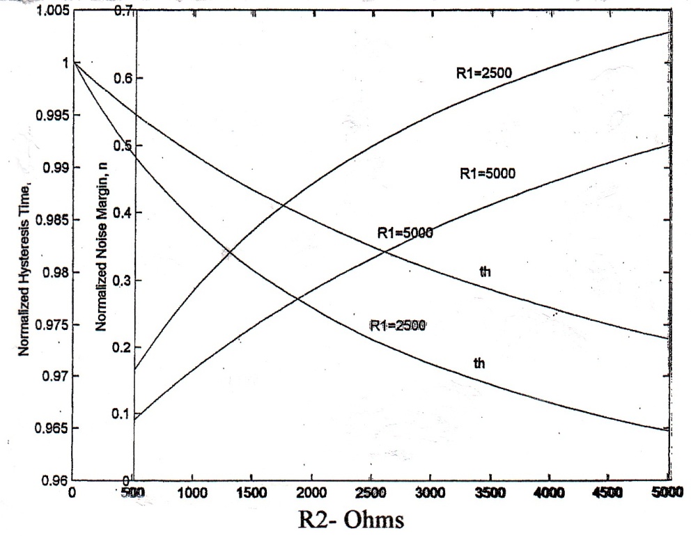
Fig.10-10 Optimal design of Schmitt trigger. The intersection of two curves establishes an optimal selection of R1 and R2 to obtain maximum N.M. and minimum th.
10.1.2.2. Differential Amplifier: A general form of op/amp using two inputs is shown in Fig 10-11.
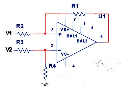
Fig.10-11. A general form of op/amp with two inputs
In practice R3=R2, and R4 =R1, in that case Vo is given by (see problem section):
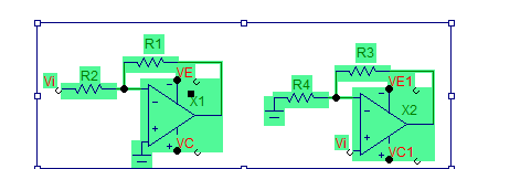
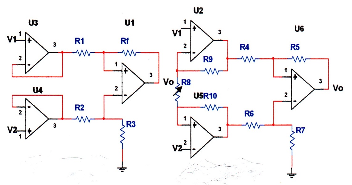
10.1.2.3. Instrumentation Amplifier: Above difference amplifier is usually used with two buffers preceding the two inputs to provide higher input impedances as shown in figure 10-12 (a, b). Figure 12(b) provides adjustable gain.
 (a) (b)
Fig.10-12. Instrumentation amplifier (a) with buffer, (b) with buffer and adjustable gain
For figure 10-12(a) with R1=R2, Rf =R3
in addition, for figure 10-12(b) with R9 = R10, R4=R6, R5=R7, Vo is given by (see problem section):
In addition to instrumentation amplifier, as noted earlier, op/amps are used extensively in industries for monitoring sensors output which will be discussed shortly. We close this section by mentioning some of the important electronic applications of op/amps, interested readers should consult references provided at the end of this chapter for further information, and these applications are:
- Implementation of active filters
- Design of oscillator
- Gyrator (an impedance converter, converting a capacitor to an inductor).
- NIC (negative impedance converter)
- A/D and D/A converter
- Integrator and differentiator
- Use of op/amps to solve differential equations
10.2. NON-CONTACT SENSORS
Industrial instrumentation relay on sensors to monitor and control the process. In the following sections, basic principles of most commonly, used industrial sensors will be discussed with several applications and practical examples. In addition, a complete list of modern and up to date sensors will be included along with several references at the end of this chapter for interested readers.
10.2.1. Temperature Sensors: Three temperature sensors and one integrated semiconductor circuit are used in industrial applications to measure the temperature.
10.2.1.1. Thermocouple: Two different metals joined at the ends and maintained at two different temperatures, generate electrical current as shown in figure 10-13.
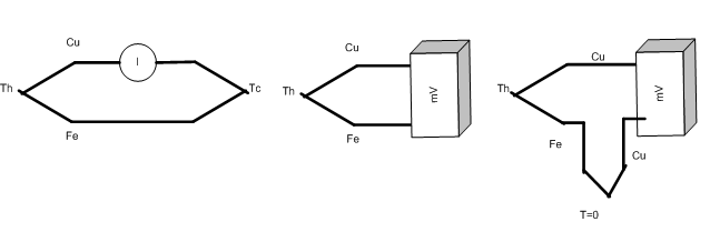 (a) (b) (c)
Fig. 10-13. Principle of a thermocouple (a) current version (b) voltage version (c) voltage version with cold junction at zero degree with copper to match to the voltmeter terminal
Note that electrical junction refers to connection of two dissimilar metals. Thus, voltmeter in figure (b) will read m V with error because iron – copper constitute a junction. To compensate for this error a second junction with a similar metal (cu in this case) is used to match to the input terminal of the voltmeter, but this junction is held at zero degree as a reference temperature. This version is used most often in laboratory environment. Version (b) is used in industrial applications.
Voltmeter reading is given by:
is Seebeck coefficient, it can be expressed as:
It is the slope of the V-T curve, usually tabulated for different types of thermocouple or it can be read off the chart as shown in figure 10-14, it is usually in mV/T.
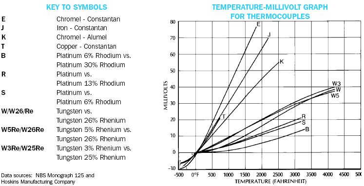
Fig.10-14.Some commonly used thermocouple characteristics [1]
As seen from these graphs, thermocouple outputs are linear functions of temperature, but very small, in mV ranges. Thus, op/amps are used extensively for signal conditioning. Figure 10-15 shows a type E thermocouple for monitoring tank temperature. Readers are requested to analyze this circuit (see problem section).
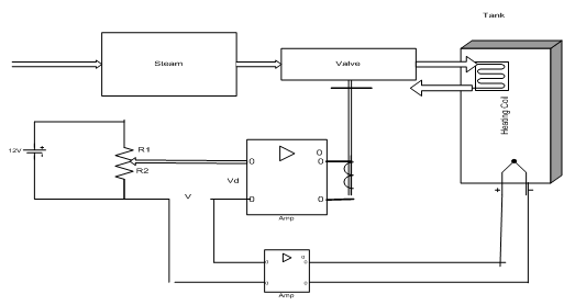
Fig.10-15 A thermocouple is used to monitor the temperature of a tank
Thermocouple outputs can also be read directly using digital voltmeter in mV range and connecting the thermocouple through an adapter to a voltmeter as shown in figure 10-16.
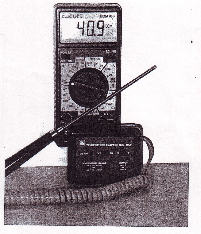
Fig.10-16 Direct temperature measurement using thermocouple with a digital voltmeter
10.2.1.2. Resistance Temperature Dependent, (RTD): This device is based on the variation of resistance with temperature according to following equation
Figure 10-17 shows R-T relation for some RTD materials.
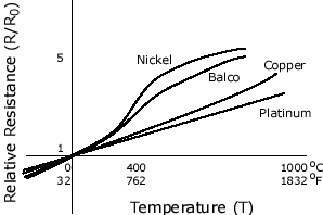
Fig.10-17. Resistance-Temperature relationship for some RTD Materials [2]
It is seen from this figure that for small variation in temperature, R can be taken as a linear function of temperature and in that case above equation reduces to a simple linear form as following:
Rh = Rc (1 + T) (10- 18)
is temperature coefficient of the wire (see table 10-1) and T is the temperature difference, Th – Tc. Care should be taken on using the unit for temperature, it must be consistent with the unit of . The cold resistance, Rc, or the reference resistance of the wire is given by equation (10-19) (also refer to problem section).
is the specific resistance, L is the unwounded length, and A is the cross section of the wire. Figure 10-18 shows one application of RTD in remote process control. Due to small change in the resistance, RTD is usually used in the one arm of a Wheatstone bridge as shown in the figure. In that case, it is important that the extra wire resistance must be accounted for in the calculation and calibration of temperature (see problem section).
Table 10-1 Temperature coefficient for selected wires
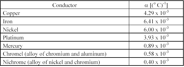
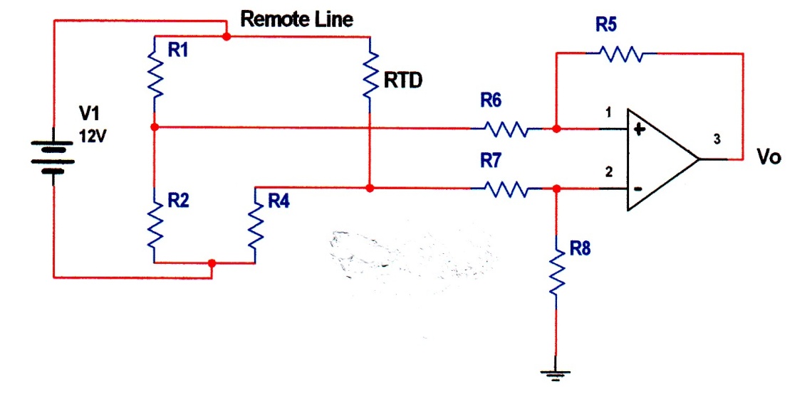
Fig.10-18 Remote sensing of temperature using RTD
10.2.1.3. Thermistor: In contrast to thermocouple and RTD, thermistors are used at low temperature. Semiconductor thermistors are based on the release of electron-hole pair upon the application of temperature as shown below:
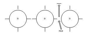
Fig.10-19 Principle of semiconductor thermistor
As temperature increases more electron-hole pair is generated, therefore, the resistance of the device will decrease. The decrease in resistance is highly nonlinear and the device is very sensitive to temperature as compared to other temperature sensors shown in figure 10-20 [3]
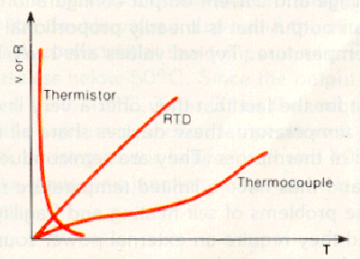
Fig.10-20 Variations of resistors/voltage of three temperature sensitive sensors
Due to its nonlinearity, thermistor modeling becomes very difficult. One mathematical description is given by:
T = Degree Kelvin
R = Thermistor Resistance
A, B, C = Curve fitting constants for the given device
For most practical and non-steep curve the resistance can be approximated by following equation;
Where K and β are geometry and material constants respectively. Exponential description can also be written as:
Again, K and β have the meaning as in equation (10-21).
The sensitivity of thermistor at low temperature makes it attractive for biomedical and electronic applications. In addition NTC thermistors such as semiconductor devices can be used to compensate for the resistance changes of the electronic circuitry to keep the overall resistance and thus, the nodal voltage constant. Figure 10-21 shows schematic of a black and white monitor in which two thermistors are used to keep the nodal voltages constant (see problem section).
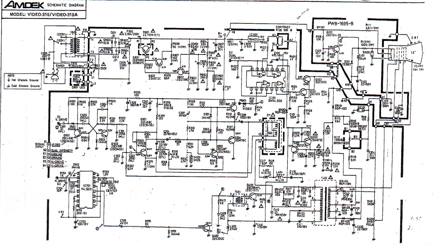
Fig.10-21 Schematic of a black and white monitor using two thermistors, TH601, and TH301 for voltage regulation (Courtesy of Amdek Corporation)
NTC thermistors are manufactured in a variety of sizes and configurations as shown in figure 10-22. Disk type thermistors are sometime mistaken for capacitors, but a simple resistance measurement should resolve this problem. Advances in new technology have now created a monolithic chip type thermistor, which will be discussed in the next section.
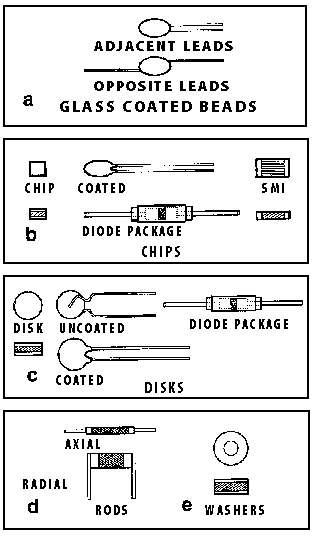
Fig.10-22.Some common types of thermistors [4]
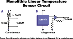
10.2.1.4. IC Temperature Sensors: A recent innovation in thermometry has created integrated circuit temperature transducer. They are manufactured in two different types, current mode and voltage sensor mode as shown in figure 10-23. The basic principle lies in the change of base-emitter voltage with temperature. They provide linear output voltage or current with temperature. Except for the fact that they offer a very linear output with temperature, these devices suffer from self-heating, fragility, limited temperature ranges, and require external bias voltage. Nevertheless, they are very convenient to use.
 |
(a) (b)
Fig.10-23.Two types of IC temperature sensors (a) current mode, (b) voltage mode
Figure 10-24 shows one application of current mode AD590 connected to the inverting input of AD311 sensing the temperature of heating element. AD590 is positioned directly on the heating element. Reference temperature is set on non-inverting input terminal 2 using Reset.
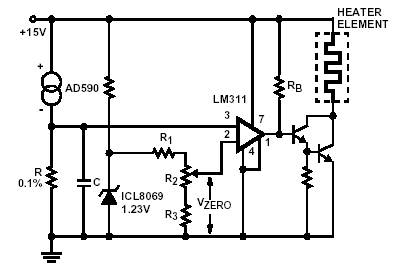
Fig 10-24 A temperature control circuit using monolithic temperature transducer[5]
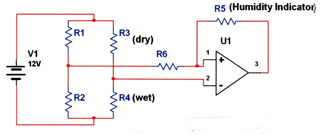
10.2.2. Humidity Sensors: Moisture content of air has significant effects in manufacturing, in warehouses, in environment, tuning musical instruments, gardens, and almost in every aspect of our daily lives. Thus, its measurement and control must be given serious consideration. In this section, several types of humidity sensors will be considered in details with several examples for their implementations. Controlling humidity remains the subject of process control and readers are requested to refer to the textbooks on this matter. Before explaining several types of humidity sensors, it is important to define absolute and relative humidity and their relation to temperature. Absolute humidity is the ratio of the mass of water vapor to the volume of air or gas. It is commonly expressed in grams per cubic meter (g/m3). It is used usually in industries such as drying textiles, paper, and chemical solids. Relative humidity (RH) refer to the ratio of moisture content of air to the saturation moisture level at the same temperature and pressure, it is expressed in %. This is the humidity we are accustomed to it. Thus relative humidity is temperature dependent, for a given temperature there exits comfort humidity for human body as shown in table 10-2 [6].
Table 10-2 Comfort Temperature
______________________________________
Temperature (C) Humidity (%)
______________________________________
39 70
34 65
31 60
29 55
________________________________________
There are three types of humidity sensors; resistive, thermal conductivity, and capacitive sensors.
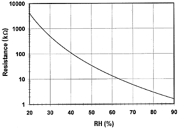
10.2.2.1. Resistive Humidity Sensors, (Hygrometer): Resistive humidity sensors are non-connected strip of thin wires positioned on a conductive polymer, salt, or treated substrate figure 10 – 25 (a). Upon absorbing moisture, the conductivity of polymer increases, thus the resistance of the strip decreases. The change in resistance is usually nonlinear as shown in figure 10-25 (b) which can be linearized by signal conditioning for direct meter reading.
(a)
 |
(b)
Fig.10-25 Hygrometer (a) Physical layout (b) Exponential response [7]
The exponential response can be expressed by following equation:
K and β are curve-fitting constants depending on the geometry and material of the sensor.
Measurement of humidity using resistance is very simple. In principle, the sensor can be connected in one arm of a full bridge circuit and direct reading of RH can be obtained after signal conditioning. One such scheme is shown in figure 10-26. Note that an AC voltage with excitation frequency of about 30 Hz to 10 kHz is required since a DC bias will polarize the polymer.
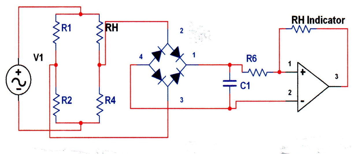
Fig.10 -26 Implementation of resistive humidity sensor
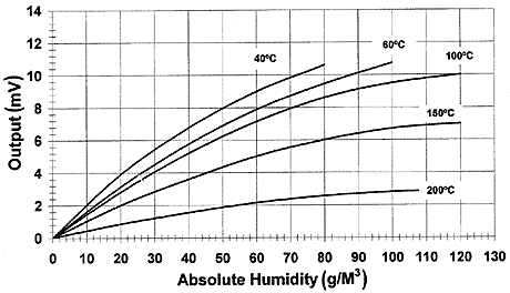
4.2.2.2. Thermal Conductivity Humidity Sensor, (Psychrometer): These sensors are used to measure absolute humidity. They consists of two temperature sensing electrodes or probes such as RTD or Thermistors one of which is hermetically encapsulated in dry and constant temperature and the other (wet electrode) is exposed to forced air flow, about 2m/s. As air flows, the temperature difference between two probes decreases, signal conditioning can be used to convert the temperature change to electrical energy. A simple resistive network using two thermistors providing 0-20mV equal to the range of 0-130g/m3 humidity at 60 degree is shown in figure 10-27 (a, b). Note that bridge is biased with DC voltage source. Note also that due to thermistor nonlinearity the output voltage is also nonlinear and is affected by temperature. Thus signal conditioning and linearization is required so that meter will indicate absolute humidity directly.
(a)
(b) |
Fig.10 -27 Absolute humidity measurements using thermal method (a) A simple bridge network using two thermistors, (b) Effect of temperature on output signal[7].
10.2.2.3. Capacitive Humidity Sensors: Some dielectric materials such as polymer or metal oxides are sensitive to moisture; if placed between two conductive plate can change the capacitance of the plates and thus can be used to measure the relative humidity, RH. Direct indication of RH can be obtained after signal conditioning. The capacitance of a parallel plate is given by;
= Permittivity of free space, 8.85 x 10⁻¹² F/m
= Relative permittivity of dielectric material
A = Common area of conductive plates
d = Distance between two plates
r is the only moisture dependent parameter in this equation. Thus, it becomes very easy to relate the capacitance changes to relative permittivity changes. For a capacitance ranging between 100-500pF the change could be about 0.2-0.5 for 1% RH change. The change in capacitance can be made linear using monolithic signal conditioning integrated circuitry. The most widely used signal conditioner incorporates a CMOS timer to pulse the sensor to produce a linear output as shown in figure 10-28. The on board sensor signal conditioning now becoming more popular and practical due to their high reliability and linear voltage output. The reader is referred to consult the reference at the end of this chapter [8].
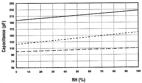 |
Fig. 10 -28 Output of an integrated capacitive sensor using CMOS technology [7].
10.2.3. Ultrasonic Sensors: Certain crystalline structures such as quartz (SiO2) if cut at proper angle and orientation can exhibit some interesting properties. If these crystals are subject to electric field, they will set in to vibration modes and produce ultrasonic wave. The effect is reversible one. That is upon the application of ultrasonic wave or mechanical strain, they will generate electric field. The process is shown symbolically in figure 10- 29. These crystals are called piezoelectric materials.
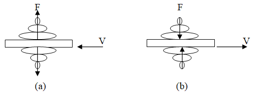
Fig.10 -29 Symbolic representation of piezoelectric crystal principle
(a) Application of electric field produces ultrasonic wave. (b)Application of ultrasonic wave produces electric field
They are 20 of 32 crystalline elements possessing piezoelectric effects. Some common elements are quartz (SiO2), LiNbO3, and GaAs. Recent trends in research have resulted in the development of thin film piezoelectric materials. Table 10-3 shows most common thin film materials used for piezoelectric applications.
Table 10-3 Some Thin Film Piezoelectric Devices and their Applications [9]
________________________________________________________________________________________
Applications Piezoelectric Materials
_____________________________
ZnO AlN PZT
____________________________________________________________________________________________
Pressure sensors +
Acoustic resonator + +
Accelerometers +
TV VIF + +
SAW + + +
Actuator + +
________________________________________________________________________________________________
Piezoelectric materials have numerous applications, which will be discussed shortly. One historical example involves their use in the production of audio from phonograph shown in figure 10-30.
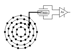
Fig.10 -30 Use of piezoelectric device to convert mechanical vibration to audio.
Different groove depth produces different acoustic wave
10.2.3.1. Theory of Piezoelectricity: Characterization of piezoelectric effect is complicated and requires stress-strain and electric depolarization analysis. An excellent treatment is found in references [10, 11]. Following is a brief description to families the reader to this exciting field so that they will not mistake this effect with capacitive or ferroelectric phenomenon.
Consider a simple molecular structure of quartz crystal shown in figure 10-31.
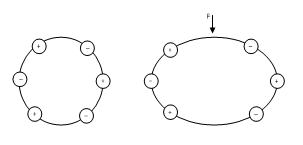
Fig.10 -31 A simple molecular structure of quartz
(a) Model at equilibrium (b) Application of central force
In equilibrium crystal, strain force is balanced by internal polarization force. When this equilibrium is disturbed either by application of external electric field or external mechanical stress, oscillation will be created to return the structure to its initial state. If the external force is from electric field (applied voltage), a displacement will occur, but if the external field is from a mechanical displacement (vibration), an electric field will be produced. There is a direct relation between electric flux density, D, and stress, T, also between strain and electric field. These relations are expressed in the following equations:
D = ε E + d T (10-25)
S = d’E + sT (10-26)
D Electric flux
ε Permittivity
E Electric field
d, d’ piezoelectric coefficients
T Stress (Force/Area)
S Strain, L/L
s Inverse of Young’s modulus of elasticity (T/S)
Equation 10 -25 indicates that stress, T, creates electric flux. Equation 10-26 indicates that electric field, E, creates strain, S. If there is no stress, equation 10 -25 reduces to:
D = E (10-25 a)
A familiar equation to most electrical students. On the other hand, if there is no electric field, E, then equation 10-26 reduces to
S = sT (10-26 a)
A familiar equation to most mechanical students. Thus, it is clear that external force, T, or electric field, E, have additional contribution to electric flux and strain in piezoelectric materials. In addition, it must be mentioned that piezoelectric crystals are anisotropic, meaning different dielectric properties. Thus coefficients , d, d’, can have three different values in x, y, and z coordinate system. Further complication arises from the fact that each of the above equations will have three component, x, y, and z. Following example will help to understand the above equations and their applications to piezoelectric materials.
10.2.3.2. Application of Piezoelectric Materials: Ultrasonic devices have several industrial and commercial applications. Examples include liquid level control, box sorting, accelerometer, and general detection system. Several references included at the end of this chapter for further readings. Regardless of their applications, their principles of operations follow equations 10 -25, and 10 -26. The following example will illustrate the significance of these equations.
Example 10-1:
Given: A piezoelectric configuration shown in figure 10-32
Required: Apply equation 10-25, 10-26 to evaluate the state of the device.
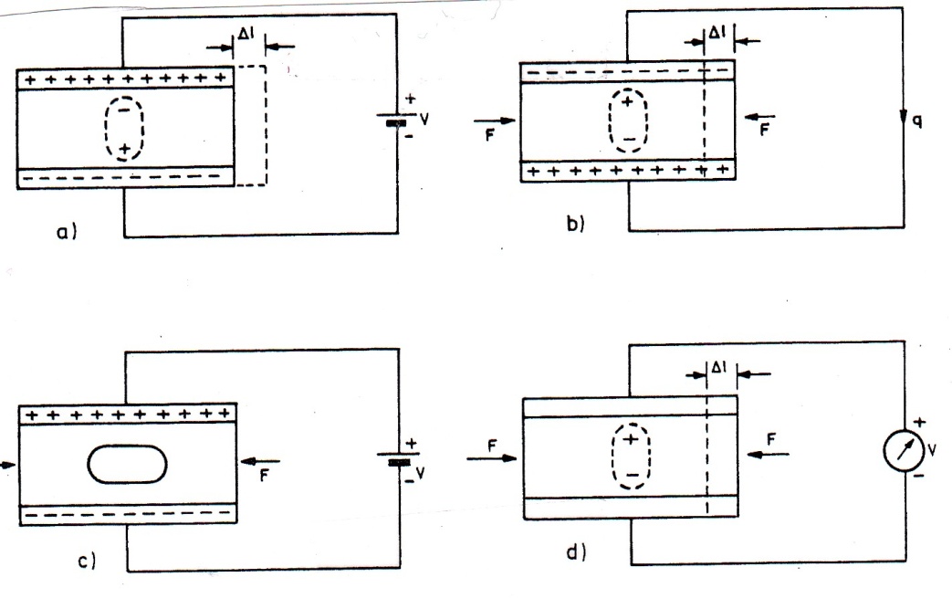
Fig.10 -32. Demonstration of piezoelectric effect
W. Welkowitz and S. Deutsch, Biomedical Instruments Theory and Design,
© 1976, Reprinted by permission of Academic Press
T=0, used for micro positioning system.
- E=0, used for measuring vibration.
- S=0, used for dielectric measurement
- D=0, used for ignition system
Solution:
Only case (a) and (b) will be considered, cases (c), and (d) will be left in the problem section.
Case (a): For this case electric field is established by V, but there is no force, so that T= 0, thus equation 10-25 and 10-26 reduces to
D = E
S = d E
Thus, there will be strain with small displacement given by:
L/L = d V/h
This last equation indicates that such a device can be used to micro positioning, for example alignment of laser mirror.
Case (b): In this case, metallic plates are shorted and a force F such as acoustic pressure is applied. Thus, equations 4-25, and 4-26 reduce to;
D = d T,
Charge obtained will be;
Thus a compression strain, S will be developed
S = s T,
This arrangement is used to measure vibration, force, pressure, and deformation.
10.2.4. Photo Sensors: Photosensitivity effect started in 1905 with Albert Einstein’s paper on photoelectric effect for which he received Nobel Prize. Since then there has been extensive research in this area and several photosensitive devices have been developed. Three types of photo sensors are in commercial and industrial use; these are photoemmissive, photoresistive, and semiconductor photo sensors. Following section is devoted to the theoretical analysis and applications of these devices.
10.2.4.1. Photoemmissive Sensors: These devices are vacuumed diode with cathode surface coated with light sensitive material such as silver, cesium, or bismuth. Light falling on the surface of cathode will release electron, which can be collected by positive anode, figure 10 -33.
Photoemmissivity effect is different for different colors. Each photon falling on the surface of a photoemmissive cathode has an energy given by:
E = hf (10-27)
h = Planck’s constant (6.62 x 10⁻³⁴ J.s.)
f = frequency of light (Hz)
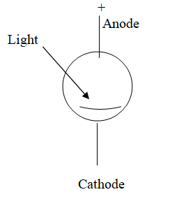
Fig. 10 -33 Principle of photoemmissive effect
Thus, different colors (f) with different energy levels will have different responses. This energy must exceed the so-called surface work function, w, of the coated cathode to release an electron, i.e.
hf > w (10-28)
w = surface work function of the cathode surface –J
The excess energy will provide enough speed for the electron to reach the anode with the speed given by:
½ mv2 = h f – w (10-29)
One special type of photoelectric devices, which is being used in the laboratories and in the researches, is photo multiplier. This device has several cathodes but one anode, figure 10-34. As the name applies, successive cathode will multiply the amount of reflected light until the anode finally collects the amplified light.
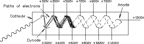
Fig.10 -34 Structure of the photomultiplier tube [12]
10.2.4.2. Photo-resistor (photo-conductor) Sensors: Some compound materials such as CdS are sensitive to light. Their resistances decrease exponentially with light according to equation (10-30). A few thin strips of these compound deposited on a flat surface exposed to light can be used to turn light on/off in residential areas, Their resistance can change from 10M Ohms to a very negligible number as seen from figure 10-35(b) :
k = geometry constant
α = material constant
I = light intensity (f-c)
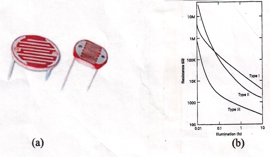
Fig.10 -35 Principle of photo-resistor device
(a)Physical layout (b) Change of resistance for three different types of materials [13]
In selecting a photo-resistor, source color must be taken in to consideration since different materials exhibit different responses. For example CdS is more sensitive to yellow-green ( = 550 nm) than to any other color. Thus, it must be used under this light condition, figure 10 – 36.
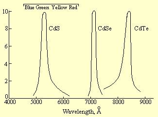
Fig.10 -36 Responses of several photo-resistors [14]
Implementation of photo-resistor is very simple. Any network, passive or active, which converts resistance change to voltage, can be used. Figure 10-37 shows one possible application, see problem section. This configuration uses Darlington Transistor to provide more current needed to turn on the relay.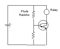
Fig.10 -37 Application of photo-resistor sensor
10.2.4.3. Semiconductor Photo-Sensors: semiconductors posses one important characteristic, in contrast to metals they are more sensitive to heat and light. Heat effect devices as thermistor were discussed in section on temperature sensors. Principle of semiconductor photo sensors is the same as thermistor, light falling on a surface of a semiconductor material will release electron-hole pairs, which can be collected by external circuitry, figure 10 -38.
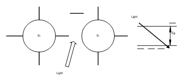
Fig.10 -38 Principle of semiconductor photo sensor
Photon energy, E, must exceed energy gap of the semiconductor material, i.e.
Ep > Eg (10-31)
hf > Eg (10-32)
Table 10 -4 Energy gap of some common semiconductor photo-sensors
____________________________________________________________________________________
Material Wavelength Energy Gap
(μm) (ev)
____________________________________________________________________________________
Ge 0.500-1.800 (0.665), 0. 8
Si 0.300-1.100 (1.12), 2.5
GaAs 0.9 1.424
InGaAs 1-1.7 0.828
_____________________________________________________________________________________
Just like photo-resistor materials, semiconductor photo-sensors have different responses for different color, thus in selecting a semiconductor for light sensing, their response curves must be taken in to consideration. Figure 10-39 shows responses of Si and InGaAs. Silicon is more sensitive at 0.8 um (red color), while GaAs is more sensitive to infrared, 1.8 um.
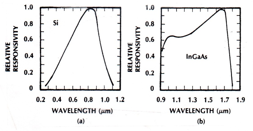
Fig.10 -39 Responses of Si and InGaAs to photon [15]
Two types of semiconductor light sensors are in common use, photo- cell (solar cell) and photo diode shown in figure 10-40.
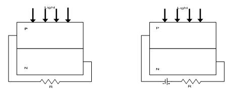 (a) (b)
Fig.10 -40 Semiconductor light sensors
(a) Photocell (b) photo diode
Note that photo diode is reversed biased to force dark current to be zero. In addition, since the efficiency of semiconductor photo sensors is low, the external resistor, R, should be chosen to match to the internal dynamic resistance of the diode for maximum power transfer as described below. Diode is characterized by:
Id ~ Is e vd/vt (10 – 33)
Is(Ig) = constant saturation current given for each diode
vd = diode voltage, not the external voltage
vt = constant thermal voltage ~ 0.026 V
This equation is plotted in figure 10-41.
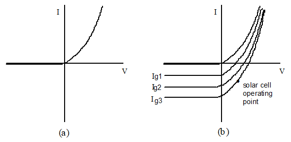
Fig.10 -41. Characteristic of semiconductor photo diode/cell
(a) Dark current characteristics (b) Illuminated characteristics,
(For photodiode operating point will be in the third quadrant)
Thus, the dynamic resistance of the diode can be determined and external resistance can be selected to match to this dynamic resistance, (see problem section).Phototransistors have one emitter and one collector leads but with no base lead. The base is exposed to light as shown in Fig 10-42 (a,b).
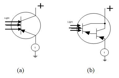
Ic = hf Ib Ic = hf1 hf2 Ib (10 -34)
Fig.10 -42 Phototransistor principle
(a) Common emitter configuration (b) Darlington connection
Phototransistors are preferred to photo diode due to their current gain as indicated by equation (10-34). Implementations of phototransistors using op/amps are shown in figure 10-43(a, b). Note that both circuits use transistor in emitter follower mode to provide high input impedance and low output impedance. Also, note that the outputs of phototransistors are fed to the non-inverting inputs of the op/amps thus providing higher impedance for the phototransistors. Op/amps also force dark current to be zero due to their high sensitivity. (See also problem section).
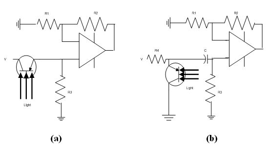
Fig.10 -43 Implementations of phototransistor using op/amps
(a) Series connection (b) Parallel connection
In concluding this section, the spectral responses of several types of photo sensors are compared in figure 10-44 with human eye sensitivity. It is seen from this figure that CdS is more in the human eye range while silicon is more sensitive to infrared radiation.
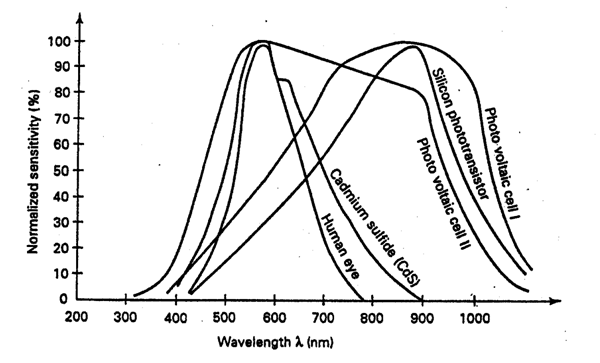
Fig.10 – 44 Spectral responses of several types of photo-sensors [13]
10.2.5. Proximity sensors: Similar to ultrasonic and photo-sensors proximity sensors are non-contact devices but are used for very short distance (cm.). Their theories and applications are also different from ultrasonic and photos sensors. Two types of proximity sensors namely inductive and capacitive sensors are in common use.
10.2.5.1. Inductive (magnetic) sensors: These sensors use magnetic core in the circuitry of an oscillator figure 10-45. The change of magnetic flux changes the inductance of the oscillator circuit thus changing the frequency of oscillation. The change of frequency can be converted to voltage for indication.
(a) (b)
Fig.10 – 45 Principle of inductive sensor
(a) Physical construction (b) Electronic presentation
The frequency of oscillator is related to inductance according to following equation;
N = number of turns on the core
= magnetic flux surrounding the core
I = current in the coil surrounding the core
A metal object near the device will disturb the magnetic flux, thus changing the inductance of the oscillator circuit and hence the frequency. The change in frequency will be converted to volt for alarm or other indication.
10.2.5.2. Capacitive (dielectric) Sensors: These devices have the same construction as inductive sensors except that they do not use magnetic cores. The core is usually sensitive dielectric material and their oscillator frequencies are affected by change in electric flux, figure 10 -46.
(a) (b)
Fig.10 – 46 Principle of Capacitive sensor
(a) Physical construction
(b) Electronic presentation
The frequency of oscillation is given by equation 10 -35, and the capacitance of parallel plate is given by equation 10 -24 as;
A dielectric object near the device will disturb the electric flux, affecting the relative dielectric constant r of the device, thus the frequency of oscillation. The change in frequency can be converted to voltage for indication or alarm.
10.2.6. Electromagnetic Sensor: (Gauss meter, Hall probe). These sensors are non-contact devices but unlike previous sensors, their operations require both electric and magnetic fields. It was demonstrated by Hall in 1879 that if a piece of semiconductor such as n or p type silicon with applied electric field placed in a magnetic field, a second electric filed perpendicular to the first applied electric field will be developed across the semiconductor, thus establishing a Hall voltage. Since its development, the device has found several commercial, industrial, and research applications, which will be discussed in the following section.
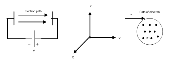
10.2.6.1. Theory of Electromagnetic Sensors: It is instructive to consider the effect of electric and magnetic field on a charged particle separately, and then discuss the combined effect. Figure 10 – 47(a) shows the effect of electric field. In this case due to electric force electrons move toward the anode in a straight line. Figure 10 -47(b) shows the effect of magnetic field. In this case, due to magnetic force electrons move in a circular path.
(a) (b)
Fig.10-47 Effects of electric and magnetic fields on a charged particle
(a) Effect of electric field (b) Effect of Magnetic field
The force due to electric field is given by:
Ey = Electric field
V = Applied DC voltage
Y = length of semiconductor
q = Electron charge, 1.6 x 10⁻¹⁹ Coul.
The force due to magnetic field is given by:
Fm-z = q vy Bx (10-38)
vy = Electron velocity in the y direction
Bx = Magnetic field in the x direction
Now, consider the combined effect shown in figure 10-48. Resulting path is not a straight line or a circle, but somewhat it is like a helix with electrons pushed to upper layer thus establishing a second electric field at top and button layer. This field or the voltage referred to as Hall voltage.
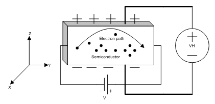
Fig.10 – 48 Principle of Hall Effect
Hall voltage can be evaluated using static condition along the z-axis as following:
Fh = Fm (10-39)
Vh = z vy Bx (10-41)
This last equation can be manipulated to obtain other parameters such as conductivity, mobility, or flux density, B. For example, mobility can be obtained as following: The velocity of the charge carrier is related to the mobility according to following equation:
vy = µ Ey (10-42)
For n-type/p-type, µn/µp should be used in the above equation. Substitution of this equation in (10-41) one obtains:
Thus the mobility, µ, can be determined from other known parameters. conductivity can also be determined according to the following equation:
σ = q µ n (10-45)
n is the carrier density. Another equation of interest, which can be derived from the above relationship, is given below (see problem section):
I = current in the sample or in the probe
A = cross sectional area of the sample
10.2.6.2. Applications (Gauss meter, Hall probe): Electromagnetic sensors have several applications. For example, they can be used to measure the magnetic flux, B. A Gauss meter or geomagnetometer operates on the principle indicated by equation 10 – 46. This device is simply a voltmeter with a Hall probe inserted in to the magnetic field to measure the magnetic flux, figure 10-49.
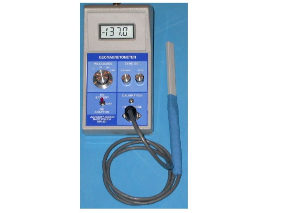
Fig.10 -49 A Gauss meter with Hall probe [16].
The probe is a piece of semiconductor material such as InSb, GaAs, or Si. Silicon has the advantage that signals conditioning circuit can be integrated on the same chip. Hall probe can also be used for monitoring the magnetic flux of induction machines. Proper operation of equipment requires uniform distribution of magnetic flux in the air gap of rotating machines. However, over a period of time (about 5-10 years), due to bearing wear, flux become non-uniform, and machine operates in an oscillatory manner. Hall probe can be inserted in to the air gap to monitor the flux distribution.
Hall probe has special applications in characterizing semiconductor material. As mentioned earlier material properties such as mobility, conductivity, and carrier density, all can be obtained using Hall probe. One such setup used in the physics lab of The University of Memphis is shown in figure 10-50. Material is mounted on the probe, inserted in magnetic field, and the desired properties are obtained using Gauss meter. Magnetization is obtained using external supply and water is used for cooling.
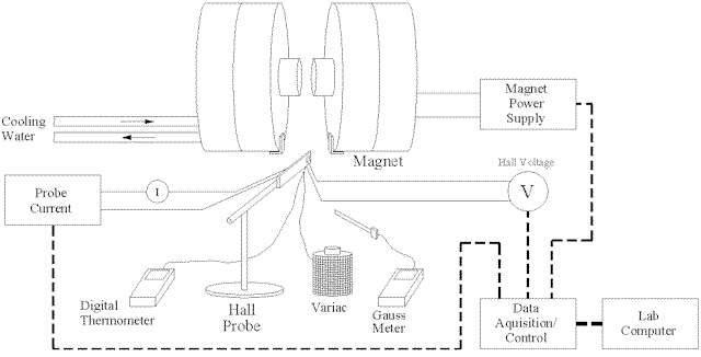
Fig.10 -50. Apparatus & equipment setup in the physics lab of University of Memphis for measuring material properties using Hall Effect devices
10.2.6.3. Specifications: A general purpose Gauss meter used in industries or laboratories should have the following specifications:
1. Range: 20 – 2000 mill Gauss 4. Portable
2. Bandwidth: 100 Hz 5. Error: 5%
3. Output: Recorder 6. Resolution: 10µGauss
10.3. CONTACT SENSORS:
Strictly speaking, contact sensors are not sensors in the context of our previous definitions. These devices sense by contacting the sensing elements, they convert one form of energy to another form such as deformation to electrical output. Two types are of interest, force/pressure and thickness/displacement measurement.
10.3.1. Force/Pressure Sensors: Force or the pressure, depending on the magnitude, can be measured by several different methods. One method using piezoelectric sensors for measuring acoustic pressure was discussed in section 4.2.3. Since pressure is defined as force per unit area, thus force can also be determined from pressure measurement. Our concern in this section, however, is the application of strain gage, a contact sensor mostly used by mechanical and civil engineers to measure the force. In that sense, this evice is not really a sensor, but measures the force by deformation as is described below.
10.3.1.1. Theory of Strain Gauge: This device is a tinny piece of wire or semiconductor mounted between two iron disks one of which is fixed and the other is subjected to the force, figure 10-51.
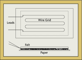 |
Fig.10 -51 Construction of strain gauge
Application of force causes the resistance of the strip wire to change; the change in resistance can be converted to force. The resistance of the wire is given by equation (10-19);
Upon the application of force this resistance becomes;
Subtracting above two equations we obtain:
For very thin wire the change in area can be neglected, thus, the total change in the resistance can be approximate as:
Gage factor is defined by:
is the strain factor. Thus knowing the gauge factor and the strain, the change in resistance can be related to monitor the force. Table 10-5 shows typical resistance and gauge factor of metals and semiconductor. Semiconductors have one special advantage of offering higher resistance.
Table 10-5 Typical resistance and Gauge factor of metals and semiconductors [11]
_______________________________________________________________________________________________
Parameter Metal Semiconductor
_______________________________________________________________________________________________
Measurement range 0.1 to 40,000µe 0.001 to 3000 µe
Gauge factor 1.8 to 2.35 50 to 200
Resistance 120, 350, 600, ….5000 1000 to 5000
Resistance tolerance 0.1% to 0.2 % 1% to 2%
Size, mm 0.4 to 150 1 to 5
Standard: 3 to 6
_______________________________________________________________________________________________
Another parameter of interest is Young’s Modulus of Elasticity. This parameter is defined as the ratio of stress/strain given by:
10.3.1.2. Implementation of Strain Gauge: Since strain gage is the change in resistance, any resistive network such as full or half bridge network can be used to measure this change. Two implementations are shown in figure 10 -52.
Fig.10 -52 Implementation of strain gauges.
(a) Half bridge network (b) Full bridge network
Full bridge network, due to its sensitivity, is preferred for measuring small changes. Strain Gage has several other applications. One such interesting application involves Automatic Weighing System given in reference [17]. For this application, four-strain Gage are used in the full bridge network instead of resistors to measure the weight of the hopper. Interested reader should consult the given reference.
10.3.2. Thickness/Displacement Measurement: In manufacturing thin material such a plastic, thickness of the sheets must be maintained within 1/1000 of an inch. This can be monitored and controlled using Linear Variable Differential Transformer (LVDT). This device is somewhat similar to electromechanical relay. Its construction and operation principle are described in the following sections.
10.3.2.1. Theory of Operation of LVDT: An equivalent circuit of a LVDT is shown in figure 10 -53(a). It consists of one primary coil and two secondary coils. Primary is subject to an input steady state sine wave of about 2 kHz@5V. Output voltage is the sum of two secondary voltages. Note that the secondary windings are in series opposition. Thus, the output voltage will be the vector sum of the two windings voltages. The induced voltage in each secondary depends on the amount of coupled flux, which depends on the position of the core. The core is free to move up/down, its position affects the amount of coupled flux, thus the amount of induced voltage as shown in the figure.
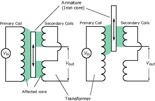
(a)
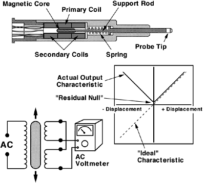
(b)
Fig.10 -53. Principle of LVDT [18]
(a). An equivalent circuit representation (b) Physical construction
For the center position, two fluxes in the secondary windings are equal, thus the output voltage will be zero, for other position there will be a net positive or negative induced voltage. Putting this in equation form, we obtain:
Core at the center: Vo = V2 –V3 = 0 (10- 53)
For core position upward: Vo = V2 –V3 > 0 (10-54)
Output voltage is a linear function of the ferrite position as shown in figure 4-54(b).
The displacement of the probe is related to the output voltage by following relation:
D = M Vo (10 -55)
Where M is the sensitivity of the device, (slope of displacement-voltage curve). Above equations are derived under the open circuit condition, i.e. unloaded device. Both load and frequency have pronounced effects on the operation of LVDT. An excellent treatment including the effect of load and operating frequency is found in reference [11]. Figure 10-54 shows the effect of load and the frequency on output voltage.
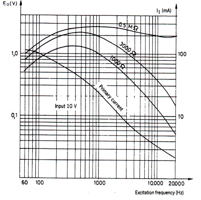
Fig.10 -54 Effects of load and operating frequency on the output of LVDT [11]
The optimum frequency for which output becomes independent of frequency is given by:
For this condition, output voltage is given by:
R1/R2: Total resistance of primary/secondary
L1/L2: Self-inductance of primary/secondary
M12/M13: Mutual inductance between primary/secondaries
10.3.2.2. Advantages: LVDT has several advantages over other displacement sensors, some are:
– Relative low cost due to its popularity.
– Solid and robust, capable of working in a wide variety of environments.
– No friction resistance, since the iron core does not contact the transformer coils, resulting in an infinite (very long) service life.
– High signal to noise ratio and low output impedance.
– Negligible hysteresis.
– Infinitesimal resolution (theoretically). In reality, displacement resolution is limited by the resolution of the amplifiers and voltage meters used to process the output signal.
– Short response time, only limited by the inertia of the iron core and the rise time of the amplifiers.
– No permanent damage to the LVDT if measurements exceed the designed range.
10.3.2.3. Specification: A good LVDT suitable for manufacturing should have the following specifications:
1. Range: 1 mm
2. Frequency: 2 kHz
3. Output voltage: 25 0mV
4. Primary impedance: <500 Ohms
5. Secondary impedance <200 Ohms
PROBLEMS
1. Refer to fig. 10 -5 comparator circuit with a constant reference voltage of Vz= 2.2 V. Minimum Iz i.e. the knee current to keep the constant zener voltage is 1 m A, and maximum Iz is 50 m A. Determine a reasonable value for R1. What is the minimum voltage at terminal 3 for light to come on?
2. Drive equation 10-4, the closed loop gain of figures 10 -6 (a, b).
3. Consider a two level comparator (Schmitt trigger) circuit given in figure 10 -8. Starting with equations 10 -8 and 10 -9, drive equation 10 -10, normalized noise margin and equation 10 -11 normalized hysteresis times.
4. Consider a general case of differential amplifier given in figure 10 -11. Show that for this general case Vo is given by:
Show that for special case with R2=R3, and R1=R4 this equation reduces to
5. Consider adjustable instrumentation amplifier given in figure 10 -12(b). Determine the voltage gain of the first stage, i.e. determine (Vo2 – Vo1))/ (V2 – V1) where Vo1(Vo2) is the output of the op/amp U2 (U5). Now use equation 10 -12 to obtain equation 10 -14, i.e. obtain overall gain of the adjustable instrumentation amplifier.
6. Refer to figure 10 -15 in which a closed loop negative feedback is used to control the temperature of a tank. Each amplifier has a voltage gain of 10. The output of the amplifier connected to the valve is 5V, and R2 = R1/11. Thermocouple is type E. Determine the temperature of the tank.
7. Consider 100 W @120 V bulb which has a cold resistance, Rc = 10 Ohms. Its element is made of tungsten which has temperature coefficient, α = 0.005. Determine its temperature when it is plugged in to 120 V outlet.
8. Refer to figure 10 -21 Amdek black and white monitor. The voltage across TH601 is measured to be 0.5 V. Using the temperature curve provided below, determine the temperature of the thermistor. Hint: Base current of transistor Q603 can be neglected.
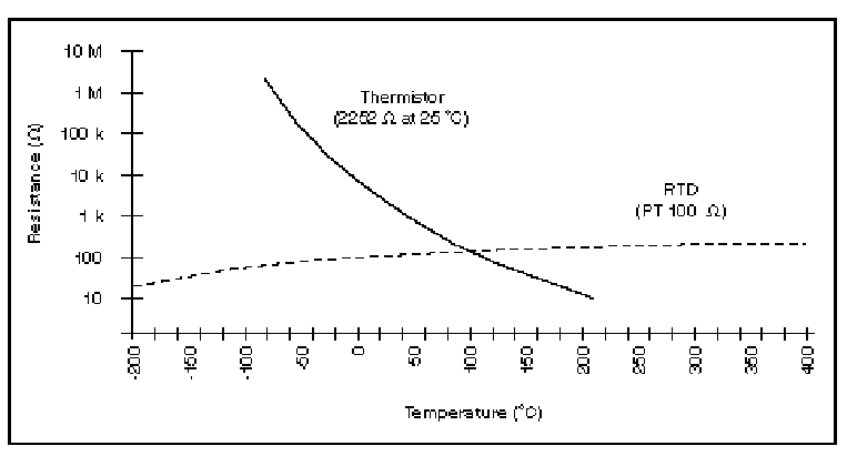
Fig 10-55 Variation of thermistor resistance with temperature (Courtesy of National Instruments)
9. Refer to figure 10 -32, demonstration of piezoelectric effect. Following the procedure outlined in example 10 -1, determine state of the device for the part (c) and (d).
10. Refer to figure 10 -40, semiconductor photocell or photodiode device. Diode can be described approximately by equation 10 -33. Due to low power level and low efficiency, the external resistance must be optimized by matching it to the internal dynamic resistance of the diode. Using above-mentioned equation, determine optimum value for the external resistance in terms of other known parameters.
11. Gauss meter often is used to measure the carrier concentration, n, in the sample. Show that n is given by equation 10-46.
REFERENCES
[1].http://www.thermometrics.com/assets/images/thermcpl.pdf#search=’thermocouple%20types%20graph’
[2]. http://www.efunda.com/DesignStandards/sensors/rtd/rtd_theory.cfm
[3]. http://www.gteck-india.com/technicalF.html
[4]. http://www.globalspec.com/cornerstone/ref/negtemp.html
[5]. http://www.intersil.com/data/fn/fn3171.pdf
[6]. http://www.pangea.org/escolapies/conforan.html
[7]. http://www.sensorsmag.com/articles/0701/54/main.shtml
[8].http://content.honeywell.com/sensing/prodinfo/humiditymoisture/catalog/c15_95_091
3.pdfttp://con
[9]. S.M.Sze, “Semiconductor Sensors”, John Wiley & Sons, Inc., 1994.
[10]. Shyh Wang, “Solid State Electronics”, McGraw-Hill Book Company, 1966.
[11]. Ramόn Palla’s-Areny, John G. Webster, “Sensors and Signal Conditioning”, John Wiley & Sons, Inc. 19991.
[12]. http://www.triumf.ca/safety/rpt/rpt_6/node21.html
[13]. Joseph J. Carr, “Sensors and Circuits”, PTR Prentice-Hall, Inc., 1993.
[14]. http://www.thiel.edu/digitalelectronics/chapters/apph_html/apph.htm
[15]. Joseph C. Palais, “Fiber Optic Communications”, Prentice-Hall1998.
[16]. http://www.gaussmeter.info/dc-gauss.html
[17]. Timothy J. Maloney, “Modern Industrial Electronics”, Prentice-Hall, 2001.
[18]. http://www.geocities.com/styrene007/sensors/SEMINAR.html
GENERAL REFERENCES
[1]. Handbook of Applied Electrical Engineering, Chapter 10.5, IEEE Press/Wiley, due for publication, 2004.
[2]. Charles Kitchin and Lew Counts, “A Design Guide to Instrumentation Amplifier”, 2nd ed., Analog Devices, Inc., 2004.