1. General Concept
1.1. Case 1. Low Frequency Analysis
1.1.1. Mathematical Method
1.1.2. Graphical Method
1.2. Case 2. High Frequency Signals
2. Methodologies
2.1. Transformer Method
2.2. Transmission Line Technology
2.2.1. Short Circuited T-line
2.2.2. Open Circuited T-line
2.2.3. Quarter-wave Transformer
2.2.4. Pure Input Resistance
2.2.5. Stub Matching
2.3. Solid State Electronics – Impedance Conversion
2.4. Antenna Impedance Matching
2.4.1. Half-Wave Dipole
2.4.2. Folded – Dipole
2.4.3. Quarter-Wave Mono-Pole
2.4.4. Balun
2.5. Microwave Antennas
2.6. Optical Lenses
2.7 Acoustical Instruments
Appendices
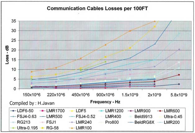
1. Communication Cables Losses Per 100 Ft.
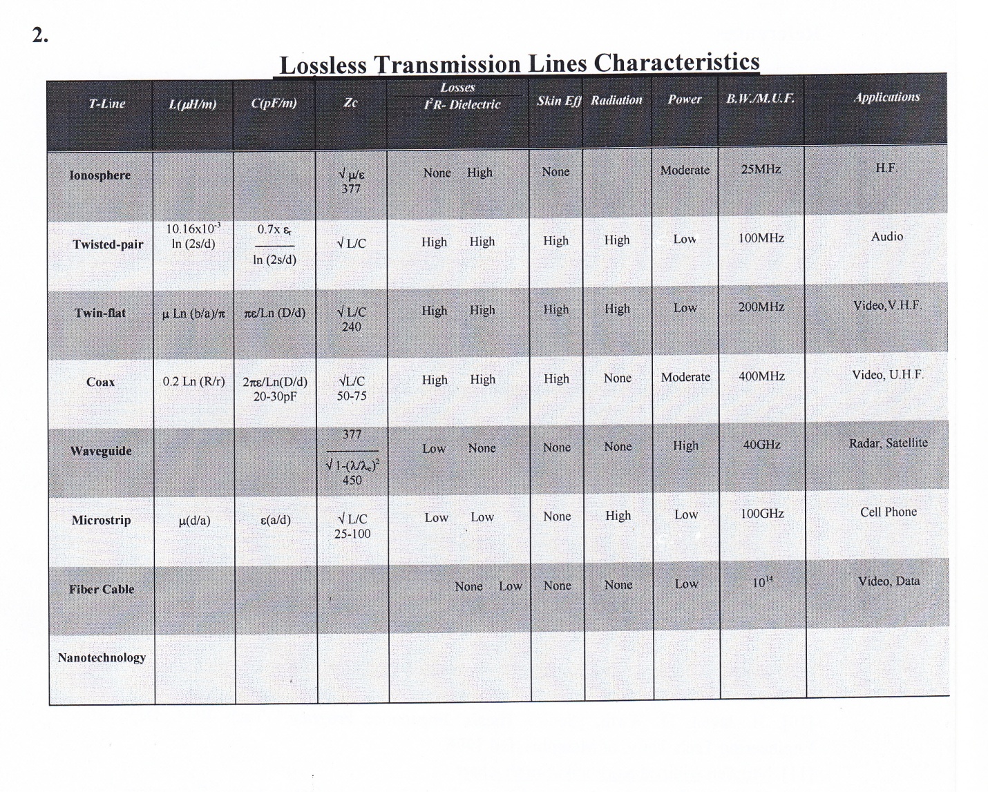
2. Lossless Transmission Lines Characteristics
References
Problems
1. General Concept
Electronic signals, in contrast to power line, are made of complex wave forms mixed with different frequencies and noise low in amplitude especially in industrial applications such as sensors outputs. This requires complicated signal processing, filtering, and amplification. Table 1 shows the approximate values of some common electronics signals.
Table 1- Approximate values of some common electronic signals
| Frequency (Hz) | Level | Signal |
| 100-20 k | 1-100 μV | Microphone |
| 500 kHz-30 MHz88-108 MHz | mV/μV | Radio waves,A.M/F.M |
| 2.45 GHz | mV | Bluetooth/Wi-Fi |
| 821-941 MHz | 50μW/m2 | Cell phones |
| 1.575 GHz | μV | GPS |
It is clear from this table that to obtain a fait full reproduction of the transmitted information, receiver will have complex tasks of; converting the frequency, filtering the noise, and amplifying the signal. This series will only discuss signal amplification by means of impedance matching techniques. Frequency conversion and filtering are covered in almost all communication textbooks.
Consider a simple circuit shown in Fig.1.
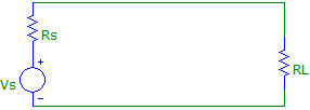
Fig.1 A simple electronic circuit
The signal generator Vs, can be considered as a received signal from the antenna, as audio signal from the headphone, or outputs from any kind of industrial sensors. The question is: under what conditions, load can receive maximum power. In other word what must be the value of the load to optimize receiver power. The answer has been provided in almost all texts books, first course in electrical engineering. Basically, it requires the determination of power in the load and maximizing it with respect to the variable, which in our case is the magnitude of the load resistance or its reactance. We outline the procedure below for two cases;
1.1. Case 1- Low Frequency Analysis: under this assumption, signal source can be considered resistive. Frequency should not overlap H.F. region. Referring to Fig.1, power in the load is calculated as follows;
![]()
There are two general methods to find the optimum value of RL, which yields maximum power; mathematical or graphical.
1.1.1. Mathematical Method:
![]()
![]()
Under this equal termination, the load voltage will be Vs/2 and the maximum load power will be;
![]()
With Rs being equal RL, source resistance voltage will also be equal to (Vs/2), and thus its power will be equal to load power. Equation (3) establishes an important electronic property for optimal signal reception. Please refer to problem section for some interesting related questions.
1.1.2. Graphical Method: We have plotted PL vs RL for Vs=1V and Rs =50Ω and Rs=100Ω with the result shown in Fig 2 for the data file given in table 2. Again, it is clear from this figure that maximum power is obtained for RL =Rs.
Table 2 – Data file for equation (4)
>> RL=0:1:400;
>> Vs=5;
>> Rs1=50;
>> Rs2=100;
>> y1=((Vs./(Rs1+RL)).^2).*RL;
>> y2=((Vs./(Rs2+RL)).^2).*RL;
> plot (RL,y1,RL,y2)
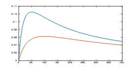
Fig. 2 Graphical method of obtaining optimum load resistance
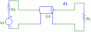
1.2. Case 2 – Higher Frequency Signals: AT H.F. (100 MHz and above) source becomes reactive due to wires leads. For example, a 50Ω source having 1μH of inductance, at 100 MHz will have an inductive reactance of
|Xs| = 2πf (1 x 10⁻⁶) ̴≅628Ω! (5)
In addition, the source impedance will be:
Zs = 50 + j 628 (6)
Thus, RL and Rs of Fig. 1 should be replaced by ZL and Zs as shown in Fig. 3.

Fig. 3 A simple reactive loads and source circuit
Under such condition load must have a susceptance part to cancel the reactance part of the source, in addition to RL = Rs. Following the same procedure for resistive source it can be shown that in this case, to obtain maximum power in the load, we must have
ZL = Zs* (7)
RL + J XC = Rs + J XL (8)
Equation (7) indicates that if the source is inductive, the load must be capacitive of equal magnitude in addition to equal resistors. This is in fact the series resonance effect as is expected. Please refer to problem section for derivation of above equations.
2. Methodologies
Several methods are available to match or to convert the load impedance/resistance to that of the source to obtain maximum power depending on the circuit configurations and the frequency of interest. The remaining of this series will be devoted to the development, theory, and the techniques of these methods.
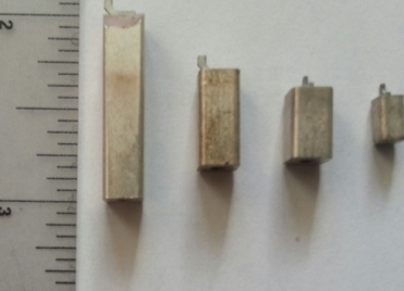
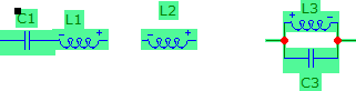
2.1. Transformer Method -Two types of transformers, which are used, for impedance matching and impedance conversion to optimize receiver’s power are shown in Fig 4.
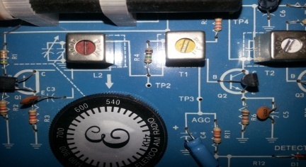
Laminated ferrite core transformers are used in the output stages of audio amplifiers to match the high output impedances of the output stages to the low input impedance (typically 4, 6, 8, and 12 ohms) of the speakers while ferrite coils are used mostly in the I.F. stages of R.F. amplifiers. Regardless which device is used, the primary object is the determination of the turn ratio of the transformer to deliver maximum power to the load. Referring to Fig 4 (a), the transformer turn ratio can be determined as follows;
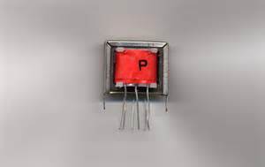
(a) (b)
![]()
(c)
Fig. 4 Transformers (a) Ferrite core transformer (b) ferrite coils, two small I.F. coils (red and yellow colors) are used in the bases of transistors for impedance conversion. (c)Transformer representation.
![]()
Using general voltage-turn ratio:
![]()
in equation (9), we obtain:
![]()
But since ![]() , equation (11) transforms to:
, equation (11) transforms to:
![]()
This impedance must match the source impedance, Zs, as shown in Fig 3. Thus,
![]()
Finally optimum turn ratio to deliver maximum power to the load becomes;
N1/N2 = √ Zs/ZL (14)
Note: Above derivation have not taken losses in to consideration. Transformer are not 100% efficient, their losses should not exceed 3% of their rated power capacity. These losses are;
1. Eddy current losses due to circulating current in the ferrite material. It varies as the square of frequency and the flux density according to following equation [1, 2];
![]()
k is a material and geometry constant.
This loss can be reduced by using laminated ferrite.
2. Hysteresis losses due to energy lost in aligning magnetic domain of the core material. It varies linearly with frequency and exponentially with the flux;
η is a constant
This loss can be reduced by selecting a good grade ferrite.
In addition to their frequency dependent losses, transformers are, in general, heavy and bulky, gradually dying out, replacing with new technology, except in power transmission.
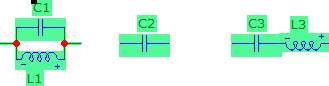
2.2. Transmission Line Method: T-lines are used for impedance matching in R.F. more efficiently where the use of transformer, due to shorter wavelength, becomes impractical. For example a short segment (5-10 centimeter) of T-lines such as RG 59 with characteristic impedance of Zc═75Ω can accomplish the same task as ferrite core transformer with negligible losses because, as will be demonstrated in the following, they can be used as a capacitor or as an inductor depending on their lengths and terminations, to optimize the power. Following is a review of T-line theory and applications for impedance matching.
Exploring T-line Theory: Consider a lossless short segment of a T-line terminated with load ZL shown in Fig. 5, which is the same as Fig. 3 except for the connecting cable with characteristic impedance of Zc assumed to be lossless.

(a) (b)
Fig. 5 (a) Some H.F. T-line (b) T-line terminated with a load impedance ZL
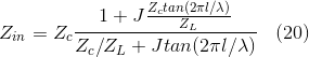
The input impedance of this line is given by [3];
![]()
l is the line length
λ is the wave length
This impedance is function of length, frequency, and the load impedance, ZL. Two types of terminations are of interest:
2.2.1. Short Circuited T-line, ZL=0; for this case Z in simplifies to
![]()
Depending on the length of the line, two cases may happen:
![]()
![]()
For this case, T-line acts like lumped element parallel or series resonance circuit depending on its length. For example, a quarter wavelength short terminated T-lines can be inserted in the base of an amplifier to obtain an oscillation without a positive feedback [4].
2.2.2. Open Circuited T- line: ZL = ∞, for this case Z in can be written as:
Or
![]()
The lumped element equivalent circuit of this line is now a capacitor.
Above cases are tabulated in table 2.
Table 2-Lumped element equivalent circuits representations of terminated T-lines
| Type of Termination | L=λ/4 λ/4˂L˂λ/2 L=λ/2 |
| Short
Open |
  |
2.2.3. Quarter-wave Transformer: One case of particular interest, which is being used extensively by R.F. and communication engineers, is the quarter-wave section terminated in any general load, ZL. For this case with l = λ/4, equation (17) transforms to;
Thus, a quarter-wave T-line acts as an impedance inverter. If the input impedance consisted of a resistance RL in series with an inductive reactance XL, it will be transferred to a resistance Rs in parallel with a capacitive reactance Xc where
Rs = Rc2/RL and X c = Rc2/XL (22)
Still another important and practical property of quarter-wave T-line can be extracted from equation (21) by matching Z in to Zs, we obtain;
Z c = √ Zs ZL (23)
The interpretation is that if we insert a quarter-wave T-line with characteristic impedance given by equation (23) between the load and the source, no matter what the nature of the load, it will be matched to the source impedance as long as geometry permits.
A word of caution: Generally Zc is considered to be a pure lossless resistor, thus the product of ZsZL must be real. This requires, except one case, (see problem section), that the load and the source must be pure resistive. In that case, we should transform the above equation to:
Rc = √ RL Rs (24)
This relation will be used in Example 1. Although our analysis is for single frequency, they can also be used for broadband matching, but the procedure is a little complicated. Interested reader should consult the reference given at the end of this series [5].
2.2.4. Pure Input Resistance: Along the loaded T – line, there is a location where the input impedance, Zin, becomes purely resistive regardless of the nature of the load. This is the most interesting part of T- line applications. This feature will be used for impedance matching as will be demonstrated in the examples to follow. Theoretically, the location, l, can be determined from equation (17) by replacing Zin with a pure resistance as;
![]()
Or……. Zin=Rin
The derivation is quite complicated, (refer to problem section). Example 1 will demonstrate its application graphically.
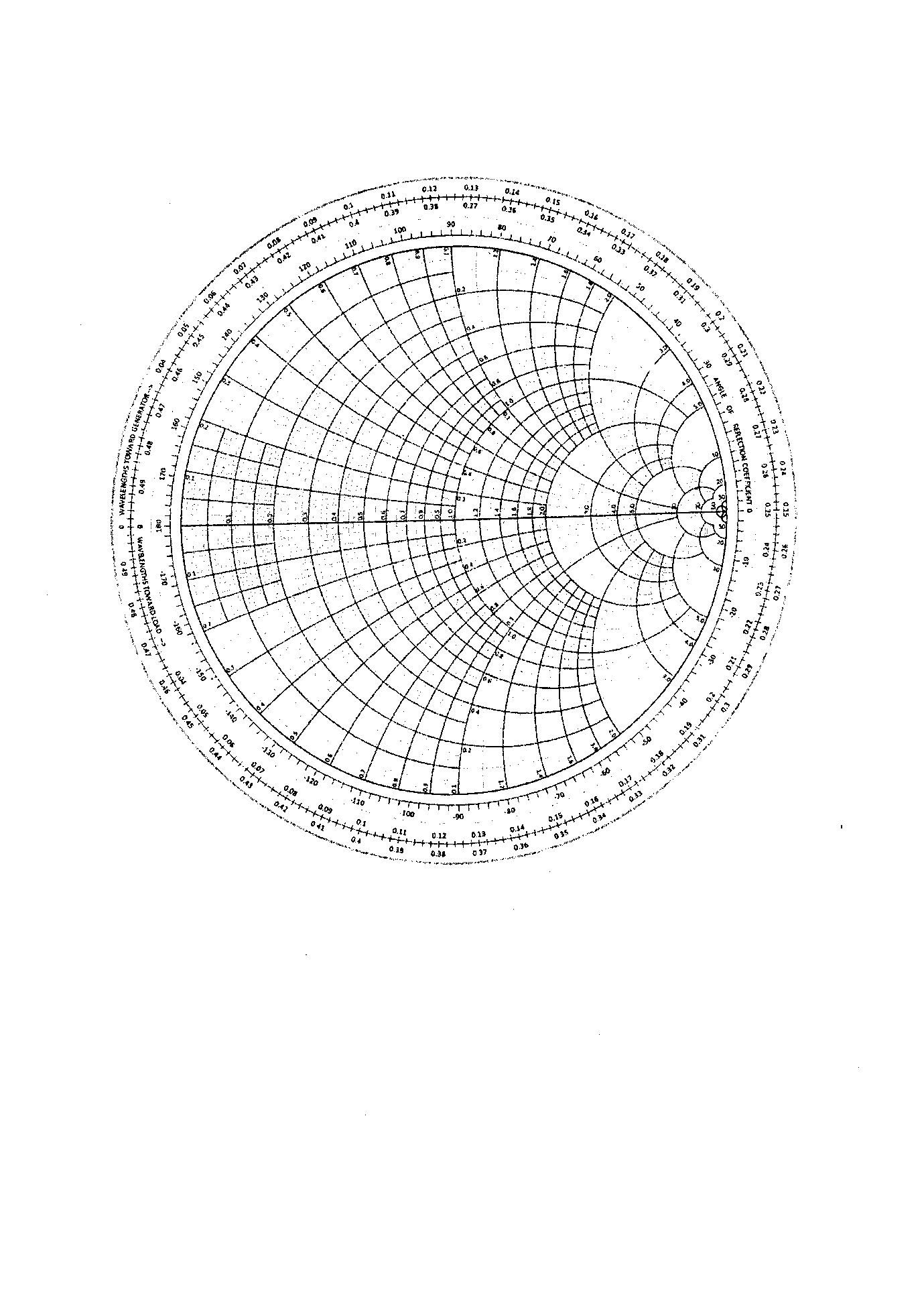
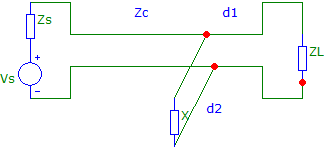
2.2.5. Stub-Matching: There are several methods such as T-Match, Gamma Match, and Omega Match of using T-lines for impedance conversion [6]. Stub matching explained in the following is the most popular one. This method has two configurations shown in Fig. 6; series and shunt stub matching. Regardless which method is used, d1, d2, Rc and x must be determined analytically, either graphically, or by simulation. Analytical method is lengthy, graphical and simulation methods are preferred. Following is a short description of graphical method referred to as Smith chart used inclusively by all communication engineers.
(a) (b)
Fig. 6 Stub matching (a) series quarter-wave matching (b) shunt matching.
Note: in (a) we have used real load, RL and real source Rs as mentioned earlier.
The Smith Chart: Introduced in 1939 is an indispensable graphical representation for impedance analysis [7]. Internet has excellent references with ample examples and descriptions [8]. The Chart is mapping the Z plane, (x, y) coordinates to Γ (reflection plane) with (u, v) coordinate according to following two equations [9].
![]()
![]()
These are the equations of two circles with changing radii and the centers; see the attached charts Fig. 7 and 8. It is indeed a challenging task to use a program to plot these circles. We have used Q basic and have obtained partial plots of these circles [10]. On these plots, horizontal circles represent the real part of Z, and the positive/negative vertical circles represent the inductive/capacitive part of the Z. Intersection of these two circles will give the real and the imaginary parts of the Z. Extreme left on the x-axis represent Z=0, the one on the extreme right with smallest radios is Z = ∞. The center of the chart presents a perfect match. The whole circle is λ/2. The chart is normalized, so that extracted number from the chart should be multiply by the reference impedance. This condensed description will be exploded with the following two examples.
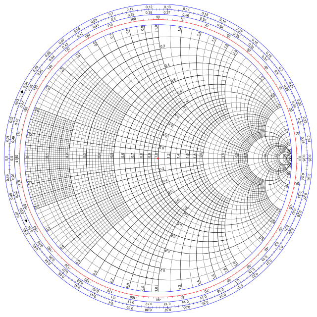
Fig. 7 Original Smith Chart [11]
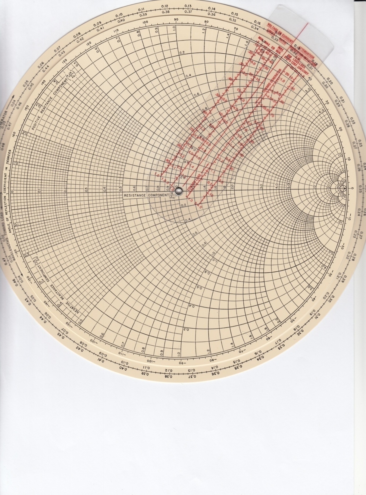
Fig.8 Mechanical Smith chart with added features [12]
Example 1:
Graphical method
Given: ZL = 100 + J 60, Zs=50, f=1 GHz
Determine: d, Zc, l, using series stub matching

Fig. 9 Circuit for example 1
Solution:
Notes: As mentioned above, series stub matching uses quarter-wave transformer. With Zs being real, it only matches the real resistances according to equation (24). Thus, we must move from the load toward the source until we locate pure input resistance, this distance will be d1. Refer to the Smith chart below. The procedure is following:
1. Normalize ZL, ZN = (100 + J 60) /50 = 2 + J 1.2, enter on S.C. point A, Fig. 10.
2. Draw a circle, radios OA, This is called VSWR circle, (it will not change as long as ZL is not changed).
3. Move around this circle C.W. (toward the source) until you cross the x-axis. Here Zin is pure resistive, d is:
d ═ 0.25λ ─ 0.21λ ═ 0.04λ
The magnitude of d is not practical on T-line. This is due to the selected frequency, shorter λ. The example is in fact calls for the use of micro strip T-line elements, which will be discussed below in example 2 for the same information given in this example. However, the above outlined procedure remains valid.
4. Read the value of the input resistance, x crossing, (3), point B, and then de-normalize it with 50Ω to obtain the real input resistance;
Rin ═ 50 x 3 ═ 150Ω
5. Calculate Rc, equation (24); Rc ═ √ Rin Rs ═ √150 x 50 ═ 86.6Ω
6. Find l l ═ λ/4 ═ 7.5 cm @ f=1 GHz
Conclusion: If we insert a coaxial cable between the load and the source with the characteristic impedance Rc ═ 86.6Ω and length 7.5 cm at a distance d1═1.2 cm from the load, the load will be matched to the source i.e. the locus of the impedance will fall immediately to the center of the chart indicating perfect match as will be verified using interactive simulation software below. Unfortunately, it is not always possible to find a coax with the exact value of Rc, but any cable with closer value will perform satisfactory. The closes cable for this case is RG-7/U, RG-22/U, RG-62/U, RG-71/U, or RG-111/U [13].
Series stub matching is not practical, cable must be cut, and terminal connections may introduce error. Shunt stub matching explained in example 2 is preferable.
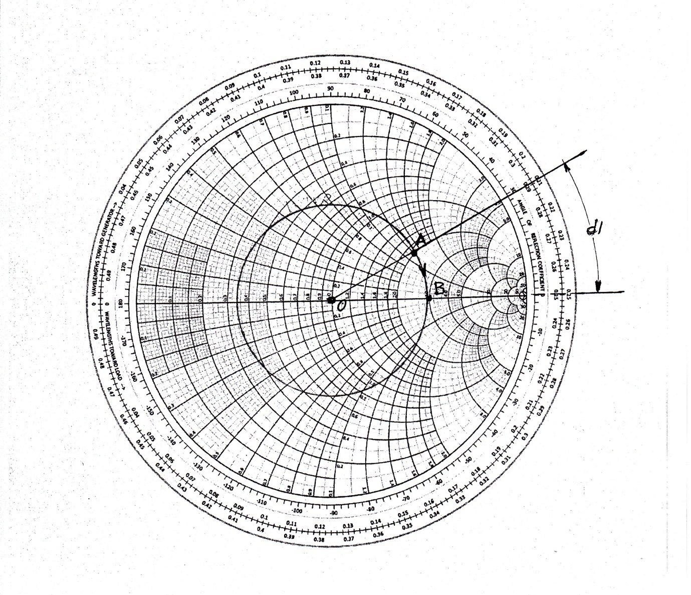
Fig. 10 Smith chart for example 1
Example 2:
Graphical method
Given: ZL = 100 + J 60, Zs=50, f=1 GHz, (same as Example 1).
Determine: d1, d2, and X, using shunt stub matching

Fig 11. Circuit for example 2
Solution:
1. Normalize ZL: ZN = 100 + J60/50 = 2 + J1.2, enter Smith chart, ZN, Fig.12
2. Draw VSWR circle, radius OA,
3. Draw line from A to O, extend until crossing VSWR circle, point B, this is YN.
Shunt matching is easier using Y instead Z. Opposite to Z is Y, Smith chart has this feature.
4. Now move C.W. toward the source until you cross the horizontal circle r = 1, point C. AT this point, the input conductance is matched to the source conductance.
YN = 1 + J 1.1
d1 = (0.374 + 0.04) λ
λ = c/ f = 3 x 10¹⁰ /1 x 109 = 30 cm
d1 = 12.42 cm
5. Now must add a capacitive reactance to cancel the inductive reactance, J1.1. This will be done by using a short-circuited T- line. Start from Y=0 move C.W. around the outer circle until you locate Bc = – 1.1/50, thus Xc= -50/1.1= -45.45.
6. Determine; d2 = 0.116λ = 3.48cm
By adding this short-circuited T-line, final locus will fall on the center of the Smith chart indicating perfect match. It is quite interesting to observe this using simulation as will be shown next.
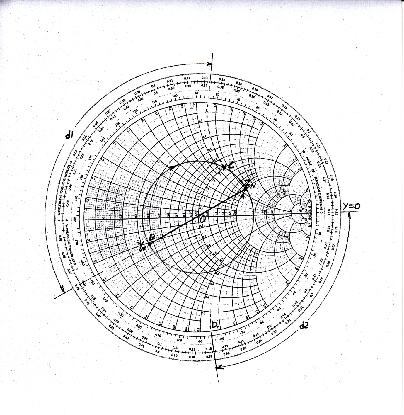
Fig. 12 Smith chart for example 2
Example 2:
Simulation
Given: ZL = 100 + J 60, Zs=50, f=1 GHz
Determine: d1, d2, and X, using shunt stub matching
Solution:
We have used MIMP and determined all the unknowns of above example by interactively tuning the elements until locus falls on the center of the Smith chart [14]. Interactive tuning of the elements is the most outstanding feature of this software. There are three screens on this program. Procedure is as follows;
Screen 1: Enter load and source impedance entry, ZL and Zs.
Screen 2: Select micro strip elements, this is d1, and d2, and x.
Screen 3: display Smith chart and tune the elements interactively until locus falls on the center of the S.C.
Please see the attached screen shots, Fig.13, 14, and 15 for verification.
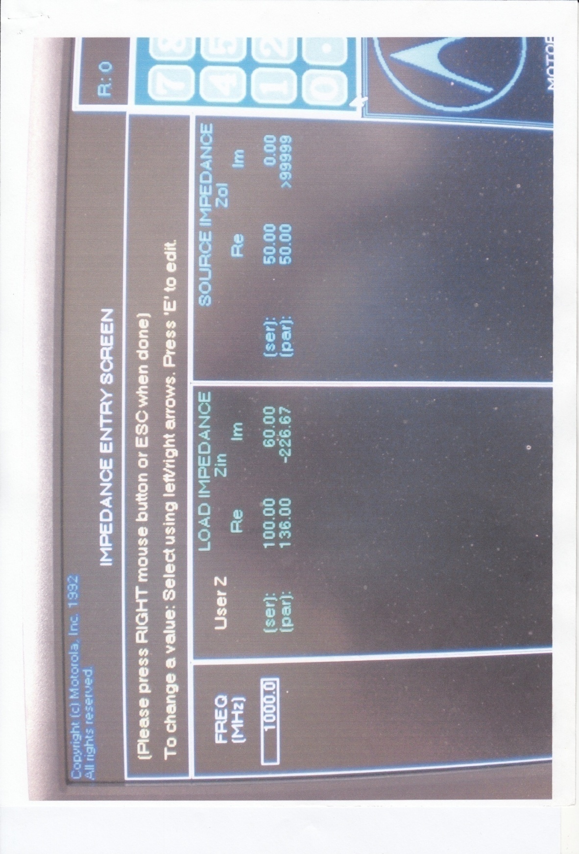
Fig. 13 Example 2- Simulation, MIMP
Screen 1- load and source entry
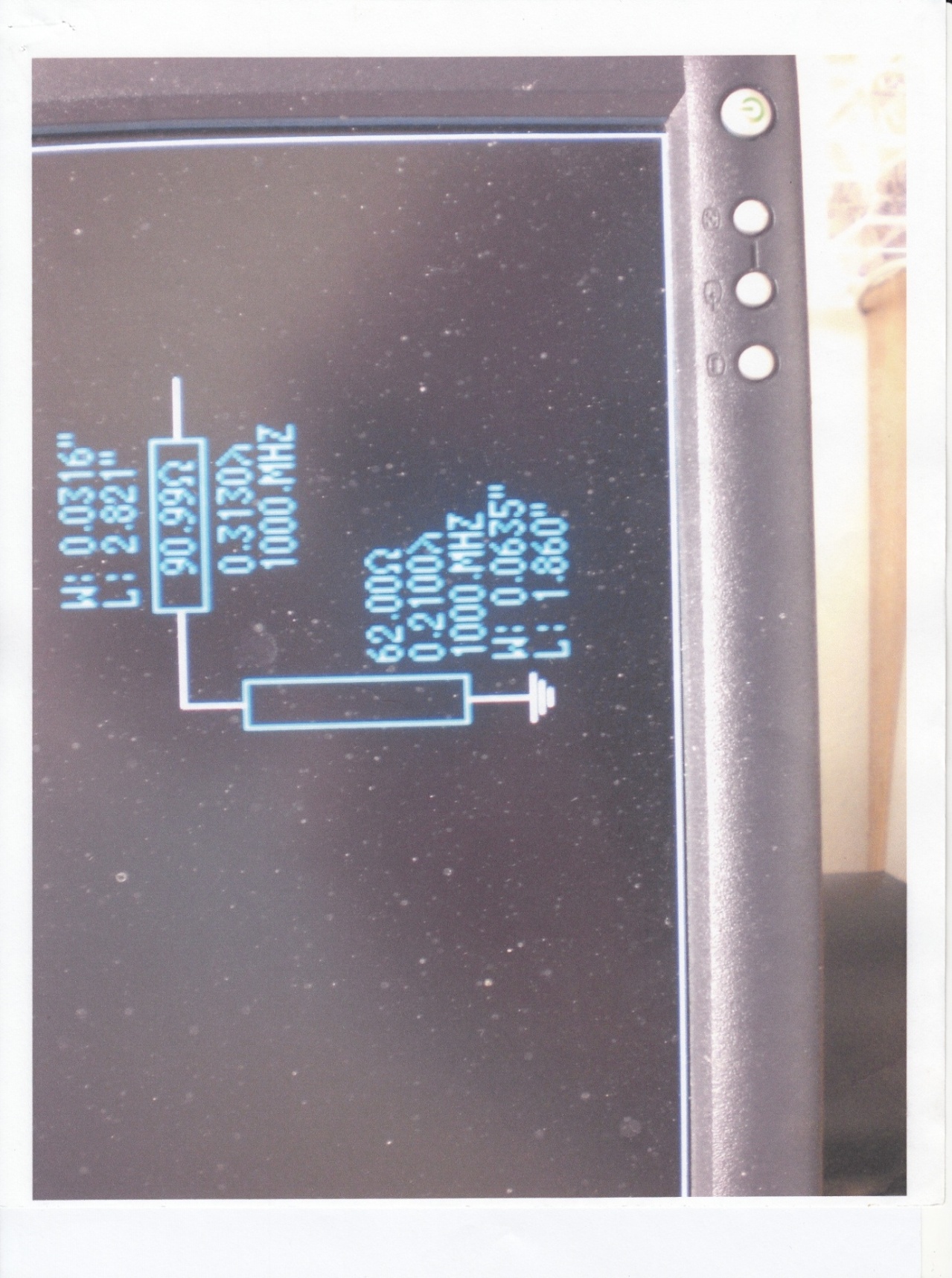
Fig. 14 Example 2 – Simulation-MIMP
Screen 2- stub entry
W/L micro strip width/length
90.99/62 characteristic impedances of strip lines
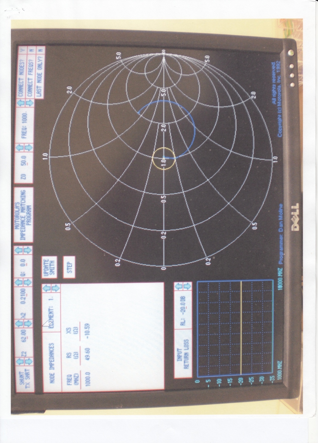
Fig. 15 Example 2-Simulation- MIMP
Screen 3
Smith chart display
Note: Final locus is on chart center indicating perfect match
Table 3- Comparison of graphical and simulation results for example 2
| Component | Graphical | Simulation |
| d1/Z | 0.414λ/50 | 0.313λ/90 |
| d2/Z | 0.116λ/50 | 0.210λ/62 |
| Xc | 45.45 | 62 |
2.3. Solid State Electronics – Impedance Conversion: Since its birth, transistor has been used in several segments of technology. Its applications include
1. as an amplifier – (analog electronics)
2. as a switch – (digital electronics)
3. As a constant current source – (power supply)
4. as an impedance converter (analog electronics)
5. as a level shifter (digital electronics)
In this series, we will consider only the impedance converter; hopefully readers are familiar with the basic principles of transistor.
Transistors are used in three different modes;
1. Common emitter
2. Common collector – (emitter follower)
3. Common base
Each mode has its own different parameters such as; input/output impedances, voltage – current gain, and power. These parameters are different for each mode. For example common collector has no voltage gain but posses high input impedance with low output impedance. On the other hand, common emitter has moderate voltage and current gain with moderate input/output impedances. Common base has no current gain but indicates negative resistance, which is used in H.F. oscillator [15]. Our primary concern will be the application of common collector (emitter follower) for impedance conversion. Consider a common collector configuration shown in Fig. 16.
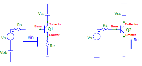
Fig 16-Common collector (emitter follower) configurations
The input and the output impedances of this configuration are given approximately by [16];
hfe is the small signal current gain; its value ranges from 50 – 200. For a nominal value of 100, if we insert a resistor Re = 10 Ohms in the emitter, the input impedance will be Rin ≈ 1 k. On the other hand, for a source resistance of 1 k, the output impedance will be 10 Ohms. It is clear from this short analysis that a common collector (emitter follower) can be used as an impedance converter, and this is in fact the case. Generally, in audio amplifier, a speaker with impedance of (4, 8, 12, 16 ohms) is inserted in the emitter. This will insure impedance conversion and thus transfer of maximum power to the speaker.
Note: Rin and Ro refers to ac quantities, thus, it is important in measuring these parameters, batries (DC) sources must be removed.
The main drawbacks of transistors for impedance matching are their low power ratings. However, with a different configuration such as push-pull or push-push amplifiers this limitation can be controlled to a certain extent [17].
2.4. Antenna Impedance Matching; Antennas are used in wireless communication to intercept the information contained in the radiated field of electromagnetic waves. Electromagnetic field contains energy; this energy will induce moving charges in the antenna, thus producing current and signals. As mentioned in the introduction section, these signals are extremely low in amplitudes, thus requiring amplifications. One way to amplify these signals is to match the antenna impedance to the electromagnetic impedance of radiated wave. Electromagnetic field is a complex science so is the antenna theory and design; they both possess impedances, which will be discussed shortly. For now, we mention that Marconi’s achievement would not be possible without a radiating instrument, the antenna [18]. Truly antennas are the most important and exciting component of electronics.
Originally, antennas were made from piece of wires in different shapes and configuration. But during the last two decades, advancement in electronic technology has opened a new exciting era in the development and designing of antennas using conducting sheets in different geometrical configurations such as microstrip and IF (inverted F ) antennas as they are used in cell phones and mobile communications [19].
Radiation principle: Consider a capacitor connected to an AC signal as shown in Fig. 17.
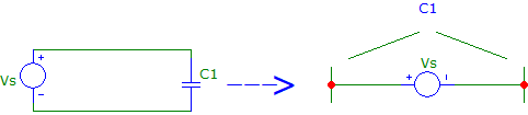
Fig. 17 Radiation principle (a) capacitor charging and discharging in an AC circuit (b) the circuit is used as radiating element
In contrast to DC, in AC circuit, capacitor charges, discharges to the air, its energy is transferred to the air in the form of electromagnetic waves. This is the energy which receiving antenna will intercept, and the information contained in the signal will be extracted. Circuit has impedance, so does the radiated wave, which is discussed in equation (31).
Note: Although we used capacitor as a radiating element, but for strong radiation they are removed. Sharper corners are better radiators. Also, note that antennas are reciprocal, i.e. the same antenna can be used for radiation and detection.
2.4.1. Half – Wave dipole: One type of antenna, which will be reshaped later for impedance matching, are shown in Fig. 18 assuming sine wave excitation.
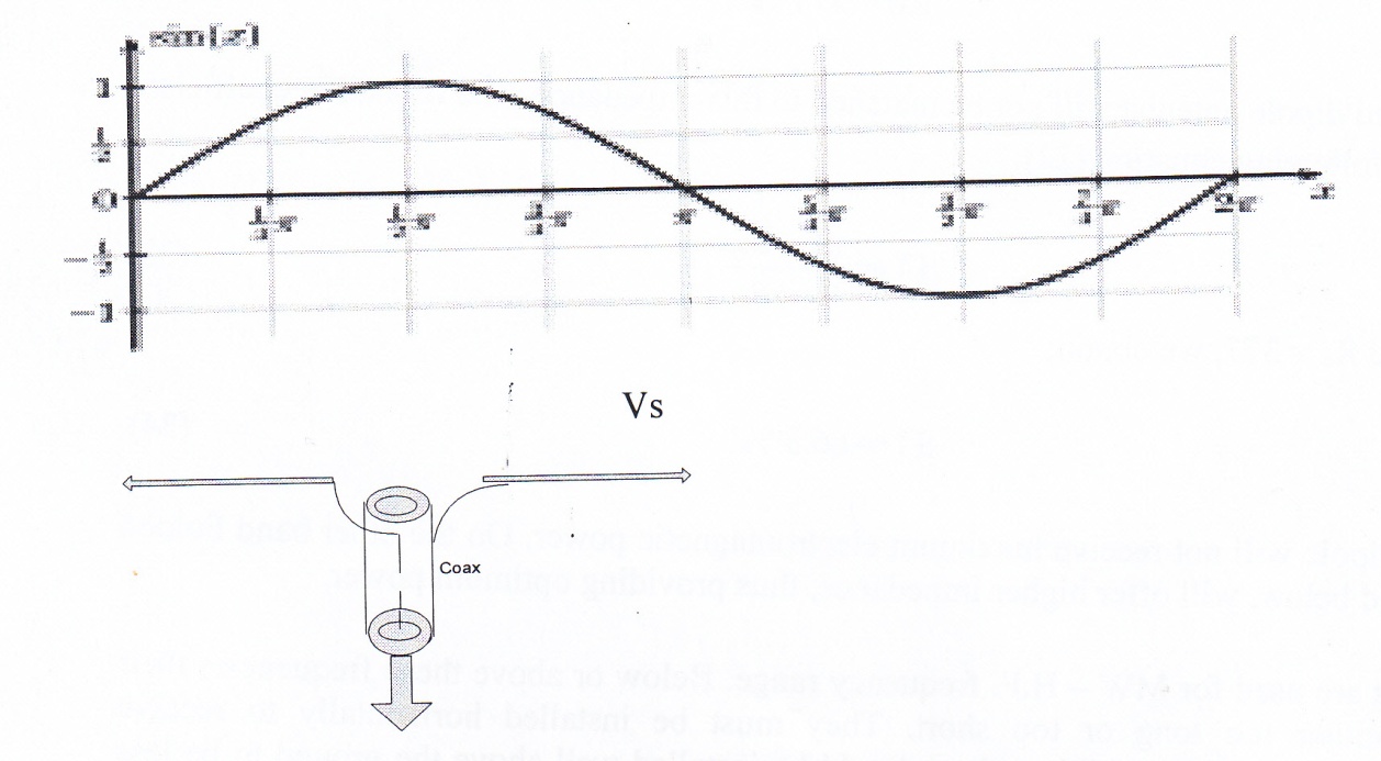
Fig. 18 – A Half-wave dipole antenna with assumed sinusoidal signal source
With assumed sine wave excitation, the current distribution along the antenna will also be a sine wave (2π = λ) as shown but the length of the dipole will be (π) or;
l ═ λ/2 (28)
λ is the wavelength given by;
λ ═ c/ f (29)
c ═ 3 x 10^8 m/sec, speed of E/W
f the frequency in Hz
Once the frequency is specified, the length of the antenna can be determined from equation (29, 28). Theoretically, every dipole is designed for a certain frequency. However, in practice, a given antenna will pick up several stations within proximity frequencies.
The radiation impedance (not the physical) of half-wave dipole is given by;
Pr is the radiated power and Io is the maximum input current. The nominal value for this resistance is about 75Ω. Its calculation is lengthy [20]. This impedance must be matched to the electromagnetic wave impedance. The electromagnetic wave impedance in free space is calculated from equation (31), [21];
Ro = √ μ o / ε o (31)
μ o permeability of free space = 1.257 x 10⁻⁸ H/cm
ε 0 permittivity of free space = 8.854 x 10⁻¹⁴ F/cm
Using these values in equation (23), we obtain;
Ro ≈ 377 Ω (32)
Thus, the mentioned dipole antenna will not be matched to this impedance. The reflection coefficient is calculated from following equation [22];
Using R r = 75, and Ro = 377, we obtain;
|Γ| ═-66.8 %! (34)
Thus, half-wave dipole will not receive maximum electromagnetic power. On the other hand Folded ─ dipole, discussed below, will offer higher impedance, thus providing optimum power.
Half-wave dipoles are used for MW – H.F. frequency range. Below or above these frequencies their lengths become either too long or too short. They must be installed horizontally to receive horizontally polarized wave. In addition, horizontal dipole antenna shown in Fig 18 should be installed well above the ground to be less sensitive to radiation from the earth’s surface and ground wave. This is why most transmitting radio stations prefer vertical quarter-wave antennas, which will be discussed later. In addition, dipole antenna installation requires poles and insulations.
2.4.2. Folded – dipole: Folded dipole usually referred to as Yagi is a paper clip shape radiator shown in Fig. 19 [23]. It is used universally at VHF covering TV channels 2-12. Above this range, we enter UHF region and dipole length becomes too short for practical applications, thus, a different types of antennas are required.
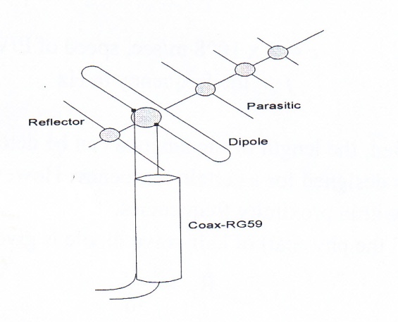
Fig. 19- A three elements array with folded dipole is used for TV channels 2 – 12
The radiation input impedance of folded dipole can be determined from equation (27) using Io/2 instead of Io which is used for regular dipole. Thus, the impedance of folded dipole will be four times the impedance of regular dipole, i.e. 300Ω. The reflection coefficient using equation (33) will be;
This remarkable improvement in the reflection coefficient as compared to the regular dipole is due to reshaping the antenna to obtain a matching impedance to that of free space electromagnetic wave impedance of 377Ω, thus receiving optimum power. In addition to impedance matching, reshaping the antenna has also a profound effect on its radiation pattern.
2.4.3. Quarter-Wave Monopole: Fig.20. This antenna is used mostly by radio transmitting stations due to its simplicity of installation and shorter length. Its length is quarter wavelength; ground is mirror image making it virtual halfway dipole. Comparing with regular dipole, we can conclude that its input radiation impedance should be half of regular dipole, i.e. 37.5Ω. Reflection coefficient will be;
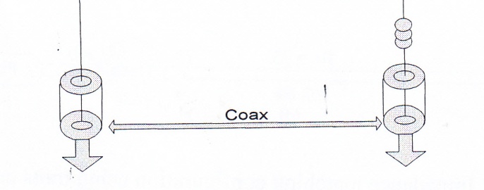
Fig. 20 – Quarter-wave mono-pole antenna
Thus, a quarter-wave mono-poles are in fact inefficient radiators. One method to increase their efficiencies is to wrap it around as shown. However, this is not an impedance matching; it merely matches its length to the wavelength, λ, since its length becomes extremely long for MW frequencies.
2.4.4. Baluns and Transformers: Baluns are a U-shaped λ/2 coaxial cables, while transformers are ferrite core devices used especially for antennas matching; coax to twin flat or vice versa Fig. 21, [4].
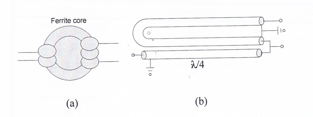
Fig. 21 Impedance matching devices (a) ferrite core transformer (b) λ/2 balun
Baluns are used to convert coax cable impedance to twin-flat, thus obtaining a balanced load while transformer is used to convert impedances balance or unbalance. Ferrite core transformers have wider bandwidth over λ/2 coaxial balun. Depending on the type of the cable, which connects the antenna terminal to the receiver terminal, there are four configurations shown in Fig. 22. 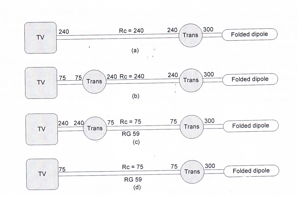
Fig. 22 Impedance matching configurations using trans or balun
From these configurations, the first two, which uses twin flat conductors, are obsolete due to high cable radiation losses. Configuration (c) is no longer available since almost all TV sets are now built with 75Ω input impedance. Also in modern technology with satellite receiver, the use of transformer after dipole becomes redundant.
2.5. Microwave Antennas: The latest microwave frequency allocation by FCC ranges from 1 GHz to 100 GHz and it is subdivided in to several bands such as L, S, C, X, and Ku bands. Table 4 shows some popular microwave frequency bands and their applications.
Table 4 – Popular microwave frequency bands
| Frequency (GHz) | Designation | Application |
| 2.45 | LS | Microwave oven |
| 2.45 | C | Wi – FiWi-Max |
| 4/6 | C | Satellite communication
Down link/uplink |
| 10 | X | Radar |
| 12/14 | Ku | Satellite communication
Down link/uplink |
At these frequencies, wavelength becomes too short, about centimeter. For example at 10 GHz, using λ = c / f, we obtain 3 cm. Using Quarter-wave antenna, its length will be one fourth of this, or 0.75 cm. The impedance matching of such antennas is not done on conventional methods discussed
so far. Their impedance matching requires special shaping the structure of the media to obtain optimum output power. One such structure is shown in Fig. 23, horn antenna. Horn antennas have their own history, in addition to their impedance matching properties; they possess high gain and wider bandwidth [25]. To determine their reflection coefficient, we need to evaluate the waveguide impedance. The rectangular waveguide impedance can be calculated from the following equation [26];
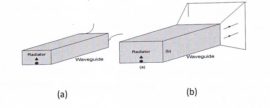
Fig. 23 Horn antenna with quarter-wave radiator
(a) none – flared waveguide (b) two – directional-flared waveguide
Z g waveguide impedance
Z o is the free space E/M wave impedance
λ o is free space wavelength
a is the wider flange dimension
For X band, (f = 10 GHz), λo is found to be 3 cm. The flange dimension a, is given in the Waveguide handbook, 2.5 cm. Inserting these values in to equation (37) with Z o =377, we obtain 471Ω. This value has been experimentally verified in our lab [27]. The reflection coefficient calculated to be;
This remarkable reduction in reflection coefficient, as compared to other radiators, is due to reshaping of the antenna as mentioned earlier. In addition to reshaping the waveguide, other impedance matching methods such as mechanical devices using screw tuners shown in Fig. 24 are used in waveguides [28]. The screw tuners, basically, act likes an inductor and a capacitor. The waveguide outputs, however, must be connected ia a microwave detector to a monitoring device such as a power meter or to a scope to observe the output while tuning the screw.
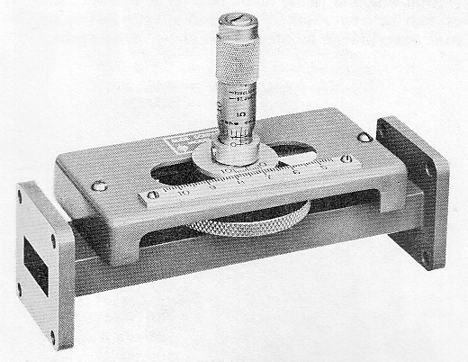
Fig. 24 a waveguide tuning stub
2.6. Optical Lenses: Optical media and T-lines have an intrinsic connection since they both carry electromagnetic wave. For example, the impedance properties of fibers can be extracted from T – lines by replacing, Z, with n, the index of refraction defined by;
n = c/v (39)
Where c/v is the velocity of wave in the vacuum and in the media respectively. Wave velocity, v, in the media is always less than c, therefore, n, is always larger than one. Some representative values of n are given in table 5 [29].
Table 5 – Index of refraction for some materials used in fibers
| Material | Index of Refraction(n) |
| Air | 1 |
| Silica (glass) | 1.5 |
| Plastic | 1.49 |
| Water | 1.33 |
One important property of optical lenses is their reflection coefficient. This can be extracted and optimized, from the equation of a loaded T- line shown in Fig. 25 as follows;
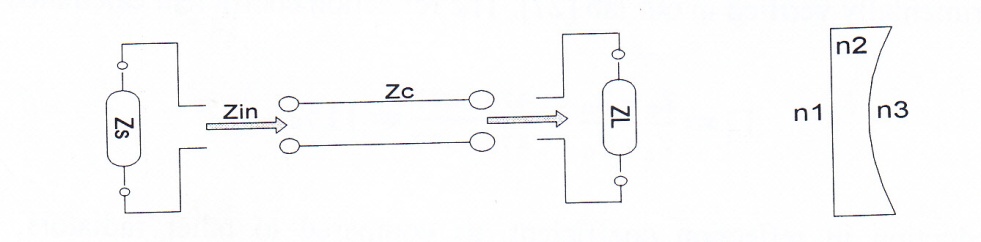
Fig. 25 Analogy of T- line to optical lens
The input impedance of this line is given in equation (17), repeated here is;
![]()
For a quarter-wave length, l = λ/4, after evaluating the limit, this equation reduces to;
Incidentally, this is the same equation (17-1). If we now terminate this impedance with a source having impedance Zs, as shown in the above figure, the reflection coefficient will be;
Inserting Zin from equation (21) in to equation (40), we obtain;
If we now replace followings [30]:
ZL → n3
Zc → n2 (42)
Zs →n1
Equation (41) transforms to:
and for optimum transmission, we require;
|Γ| = 0, or
n2 = √ n1. n3 (44)
This is exactly analogs to equation (23) of T – lines. Optical technology apply thin layer of antireflection (AR) coating to reduce the reflection, user should take care not to remove this coating by cleaning the lens quite often unless it is done with special cloth.
2.7. Acoustical Instruments – Wind instruments also use the method of re-shaping their out puts opening to match the instruments acoustical output impedance to the impedance of air, whatever it may be! Fig 26 shows two such instruments. Trumpets have narrow opening, their output acoustical impedances does not much to the impedance of the air. This is noticeable from the high frequency sound due to reflection from the air creating standing wave, while horn has very low frequency sound due to travelling wave.
![C:\Users\mm\Desktop\250px-Trumpet_1[1].jpg](http://javan.courses/wp-content/uploads/2019/05/c-users-mm-desktop-250px-trumpet_11-jpg-33.jpeg)
![C:\Users\mm\Desktop\250px-French_horn_front[1].png](http://javan.courses/wp-content/uploads/2019/05/c-users-mm-desktop-250px-french_horn_front1-png-33.png)
(a) (b)
Fig. 26 Wind instruments flared for impedance conversion (a) Trumpet (b) horn
Appendices
1. Communication Cables Losses Per 100 Ft.
References
[1]. William H. Timbie, Vannevar Bush, George B. Hoadley,” Principles of Electrical Engineering” 4th ed, John Wiley & Sons, Inc., New York 1951, pages392- 403.
[2]. George F. Corcoran, Henry R. Reed, “Introductory Electrical Engineering,” John Wiley & Sons, Inc., 1957, pages 297-303.
[3]. Edward C. Jordan, Keith G. Balmain, “Electromagnetic Waves and Radiation System,” Prentice-Hall, Inc., 1968, chapter 7.
[4]. Electronic Design, Oct.3, 1994.
[5]. H. Javan, “Noise Measure for Optimum Broadband Design,” IEE Proceedings-G, Circuits, Devices and Systems, Vol. 138, No. 1, Feb. 1991.
[6]. Constantine A. Balanis, “Antenna Theory, Analysis and Design,” John Wiley & Sons, Inc., 1982, pages 466-483.
[7]. P. H. Smith, “An Improved Transmission Line Calculator,” http://www.maximintegrated.com/en/app-notes/index.mvp/id/742Electronics, 17, 130, (Jan., 1944; also 12, 29 (Jan., 1939).
[8]. Selected references for Smith Chart with no or limited adds:http://www.files32.com/Smith-Chart.asp
http://www.maximintegrated.com/en/app-notes/index.mvp/id/742
http://www.qsl.net/va3iul/Smith%20Chart/smith.html
[9]. Edward C. Jordan, “Electromagnetic Waves and Radiation Systems,” Prentice-Hall, Inc., 1968, pages 232-140.
[10]. H. Javan, D. Wirth, “Senior Thesis, Impedance Program,” Tech 4944, Dept. of Engineering Tech, Univ. of Memphis, fall 1999.
[11]. http://en.wikipedia.org/wiki/Smith_chart
[12]. Phillip H. Smith, “An Improved Transmission Line Calculator,” Analog Instrument Co. Box 950, New Providence, N.J. 07974.
[13]. Tektronix, TDR 1503C, Metallic Cable Tester.
[14]. Dan Moline, “Motorola’s Impedance Matching Program, (1),” 6 April 1992, Version 1.0.
[15]. Richard F. Shea, Editor “Transistor Circuit Engineering,” John Wiley & Sons, Inc., New York, 1957, page 244-250.
[16]. Jacob Millman, Arvin Grabel, “Microelectronics,” 2nd ed. McGraw-Hill Book Company, 1987, page 419-422.
[17]. Ibid, pages 803-806.
[18]. http://en.wikipedia.org/wiki/Guglielmo_Marconi.
[19]. L.Pazin, N. Telzhensky and Y. Leviatan, “Multiband Flat-Plate Inverted-F Antenna for Wi-Fi/WiMax operation,” IEEE Antennas and Wireless Propagation Letters, 7: 197-200, 2008.
[20]. Constantine A. Balanis, “Antenna Theory, Analysis and Design,” John Wiley & Sons, Inc., 1982, pages 162-164.
[21]. John D. Kraus, Keith R. Carver, “Electromagnetics,” 2nd ed., McGraw-Hill, Inc., 1973, pages 378-381.
[22]. Edward C. Jordan, Keith G. Balmain, “Electromagnetic Waves and Radiation System,” Prentice-Hall, Inc., 1968, pages 215-217.
[23]. Shintaro Uda, Hidetsugu Yagi, Tohoku Imperial University, 1926
[24]. Constantine A. Balanis, “Antenna Theory, Analysis and Design,” John Wiley & Sons, Inc., 1982, pages 480-483.
[25]. Constantine A. Balanis, “Antenna Theory, Analysis and Design,” John Wiley & Sons, Inc., 1982, pages 651, 682-692.
[26]. T. Koryu Ishii, “Microwave Engineering,” 2nd ed., Harcourt Brace Jovanovich, Publisher, 1989, pages 186-189.
[27]. H. Javan, EETH 7821, “Advanced Microwave Technology,” Project No.6, Antenna Measurement, University of Memphis, Dept. of Engineering Tech, fall 2011.
[28]. Hewlett-Packard Company.
[29]. Joseph C. Palais, “Fiber Optic Communications,” 4th ed., Prentice-Hall, Inc. 1998, pages 33-38, pages 71-72.
[30]. H. Javan, EETH 7841, “Fiber Optics in Communication,” Dept. of Engineering Tech., University of Memphis, Memphis, TN 38152, fall 2000.
Problems
1. General Concept
1. A 20 Watts two channels stereo system each with 8Ω out pout impedance is to be connected to 4 speakers as shown in Fig. 36. Determine each speaker’s impedance and power rating.
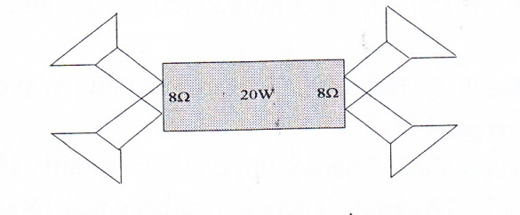
Fig. 27 Stereo system for problem 1
2. A reactive source with impedance Zs = Rs + J Xs is to be connected to a load ZL as shown in Fig. 38. Determine the elements of ZL to receive optimum power. Hint: Follow the steps presented in Case 1 for resistive source.
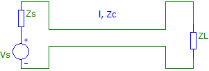
Fig. 28 Circuit for problem 2
2. Methodologies
2.1. Transformer Method
3. A 24 V, 10 Watts audio push-pull amplifier having an output impedance Ro=16Ω is to deliver maximum power to two speakers each 8Ω as shown in Fig. 39. Determine the ratios of N1/N2, N1/N3, and the power delivered to each speaker.
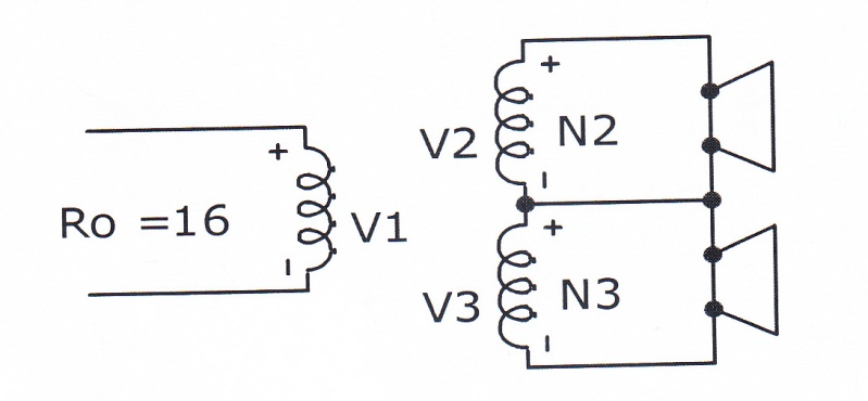
Fig. 29 Circuit for problem 3
2.2. Transmission Line Technology
4. Given general T- line equation (17), determine Zin for the following two cases, thus verifying tabulated representation in table (3).
Short terminated, l=λ/4, l=λ/2
![]()
5. Consider above equation, for what value of L, will the input impedance, Zin be equal to ZL?
This case is of practical importance for impedance matching.
6. Consider equation (17) above with a reactive load, ZL. It is shown graphically in example 1, that somewhere along the line, Zin becomes pure resistive, i.e. Zin = Rin. Determine the required length of the line. Hint: separate real and imaginary parts.
7. Consider equation (23) quarter-wavelength for impedance matching. Since Zc is generally resistive, it is necessary that both Zs and ZL to be resistive. There is one exception under which Zc will still be resistive with Zs, and ZL being reactive. Determine these impedances.
Z c = √ Zs ZL (23)
8. Given ZL = 31.25 + J 10, Zs=50, use shunt stub matching, determine d1, d2, and X. using Smith chart. Blank Smith chart is provided at the end.
2.3. Solid State Electronics – Impedance conversion
9. An emitter follower uses transformer to feed the 8Ω speaker as shown in Fig. 40. Determine the transformer turn ratio to match the speaker to the source impedance Rs of 1kΩ. The current gain of the transistor, hfe is 200.
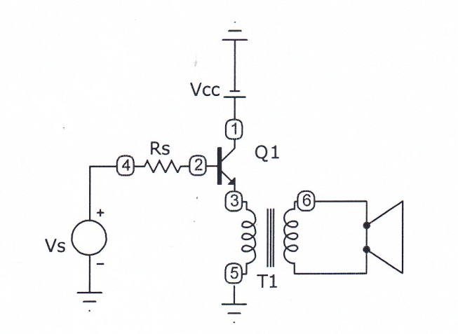
Fig. 30 Circuit for problem 9
2.4. Antenna Impedance Matching
10. Design a half-wave dipole and quarter-wave mono-pole to receive a shortwave station at f= 950 MHz.
11. A Balun is used to match the folded dipole to RG 59. Determine its length for channel 12, f=112 MHz.
2.5. Microwave Antennas
12. Determine wave guide impedance given by equation (37) for X band, thus verifying the value cited in the section. Why wave impedance is larger inside the waveguide than the free space wave impedance? Use Zo ═377Ω, f═10 GHz, a═2.5 cm.
![]()
13. In shaping the waveguide in to horn, which parameter is affected; directivity (gain) or the impedance of the waveguide?