Unintentional electronic delays spread all over this technology, yet there is not a single text or class notes explaining its sources and its effects on signal transmission in an organized format. We believe that presentation in a modular form continuously and in a sequential manner helps the students to understand the topic easily without too much confusion. It is this philosophy promoting the authors to reserve a section for this subject in this series of Class Notes. Please note that intentional delay devices such as SCR or triac in which the waveforms delayed and changed intentionally to control the speed or to obtain low DC voltages are not covered in this series.
The speed of electronic processing has now reached its stagnation point at GHz corresponding to nana second. This is not to infer that it has reached its limit. On the contrary, with advanced technology it is predicted that it will move in the upper direction. To improve the processing speed it is important to understand the mechanisms of delays. Once the sources are identified, then the remedies can be determined. It is the intention of this part of Class Notes to indentify the sources of electronic delays, and then suggest a solution. Identifications will follow in a citation method rather than proving the equations. In this respect perhaps this series can be used as a mobile hand book.
There are, in general, five types of electronic delays:
1. Transient Time Effect
2. Transistor Operation Delays
3. Propagation Delay
4. Slew Rate Effect
5. Hysteresis Time Delay
1. Transient Time Effect
This effect has been with us as early as the deification of electron. Consider a long electrode in vacuum connected to a source, assumed DC for simplicity, as shown in Fig. 1.
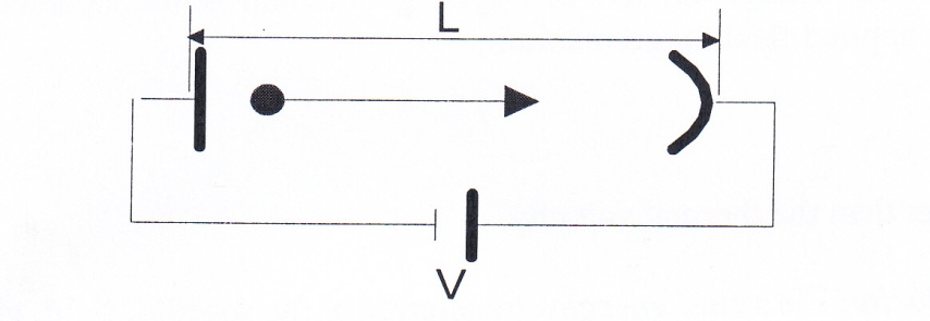
Fig. 1. Electron transient time effect.
Electron having negative charge will be travelling to the positive terminal with the delay time given by;
td = L/ν (1)
ν length of electrode
L electron velocity
A word of caution about the velocity of electron. Electron, in general, has three velocities shown artistically in Fig. 2.
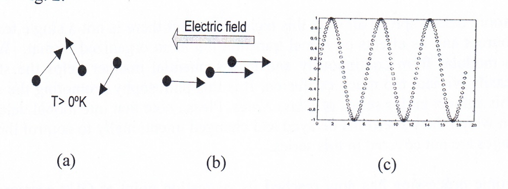
Fig. 2. Electron velocities (a) thermal velocity (b) drift velocity (c) wave velocity
1.1. Thermal Velocity due to Temperature: Electrons are in random motion; their velocities are given by [1];
1/2 m vT2 = 3√ (1/2 k T) (2)
m mass of electron
k Boltzmann constant
T temperature in Kelvin
vT = 105 m/sec. (T= 300o K)
1.2. Drift Velocity Due to an Applied Field: Electrons align with applied field, their velocities are given by:
vd = µ E (3)
µ charge carrier mobility
E =V/L, applied electric field
µ depends on the type of the charge carrier. In n-type germanium semiconductor its value is 3900 cm/v-sec. With 10V/met. applied field, in germanium;
vd = 390 m/sec.
This value is much smaller than the thermal velocity.
1.3. Electron Wave Velocity: Electrons’ energies transferred at the speed of light, given by:
vw = c = 1/√ µo (4)
µo permeability of free space, 4π x10-7 (MKS)
Permittivity of free space, 8.85 x 10⁻¹²(MKS)
In vacuum, its value is:
c = 3 x 10⁸ met/sec.
Values of these velocities are shown in TABLE 1 for easy reference.
Table 1- Electron velocities
| Name | Thermal | Drift | Wave |
| Values (met. /sec.) | 105 | 390 | 3 x 10⁸ |
Our concern should be the wave velocity, vw, because information is carried out by means of wave velocity, vw, i.e. it is the delay in vw which limits the speed of information transmission. But information, in general, is not confined in vacuum. Medium such as magnetic or dielectric materials are always present in the path of signal transmission. Their properties such as permeability µr, and the permittivity, , will reduce the speed of signal transmission, thus, we must replace speed of light, c, by following;
vw = c / õr (5)
Equation (1) now becomes;
td = L/ (c / õr ) (6)
For nonmagnetic material, µr=1, and for vacuum, = 1, in this case c will be equal to the speed of light, 3 x 10⁸ m/sec. In this case for a 30μm medium, transient delay time, td, using equation (6) will be:
td = 30 x 10-6/3 x 108 = 10 x 10-14 sec.
Corresponding to; f = 1/td = 10 THz
These are acceptable numbers, but it is for an ideal situating, the vacuum.
There are several methods to reduce the transient time delay. One simple method, as is evident from the above equations is to shorten the path length, L. This method is applied to the base of H.F. transistors as it will be shown in the next section. A second method, as is evident from equation (5) and (6) is to use material with smaller permittivity, . This will increase wave velocity, vw , thus reducing transient time.
2. Transistor Operation Delays
Depending on the modes of operations, analog or digital, transistor has two distinguish time delays which limits its high frequency response in analog operation, and switching speed in digital operation.
2.1. Analog Operation: In this mode Vbe is forward biased and Vbc is reversed biased. Transistor acts as an amplifier. Upon the application of signal (assumed small amplitude) quastatic point, Q, will swing between points A-B without entering ON or OFF regions as shown in the Fig. (3).
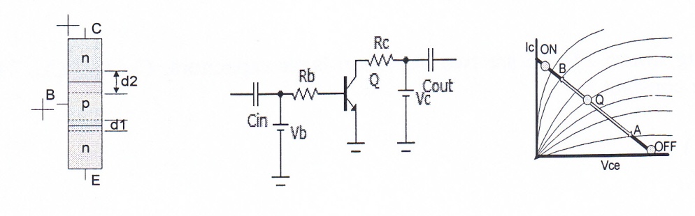
(a) (b) (c)
Fig. 3. Transistor operating in active mode
(a) Symbolic representation (b) amplifier schematic (c) characteristic curves
Transistor is restricted to swing between points A-B.
Note: H.F transistor geometry is different than shown in Fig. (a) [2].
There are two types of delays in this mode; transient time effect and capacitor charging times.
2.1.1. Transient Time Delays: Base transient time is given by [3];
tb = xb2/2 Dp (7)
xb base width
Dp base carrier diffusion constant
As mentioned earlier base width has a pronounce effect on high frequency operation of transistor. Narrow base transitory will certainly reduce the base transient delay time. In addition doping base with high diffusion constant such as GaAs will certainly reduce base delay time.
The second transient time effect, ignoring emitter junction d1, is the collector depletion region d2 shown in Fig. 3 (a). This delay is given by [3];
tc = d2/vs (8)
vs is electron saturation velocity. Collector depletion region, d2 is given by [4];
Vo built- in potential
ε dielectric constant
q charge of electron
Na/Nd donor/acceptor impurity concentration
It is seen from this equation that higher impurity concentration will definitely reduce the collector depletion region width, d2, and thus reducing the collector transient time delay. Total transient time effect will be the sum of above delays since the process is accumulative, thus
Tr = tb + tc (10)
2.1.2. Capacitors charging times: There are two depletion layer capacitors, Cbe and Cbc. These are given simply by their time constant as:
τeb = re Ceb (11)
τbc = rc Cbc (12)
These delays can be reduced by reducing emitter and collector intrinsic resistors, re and rc. In addition capacitors Ceb and Cbc can be decreased by noting that junction capacitor is given by well known formula;
A area of depletion region
d width of depletion region
Usually d1< d2 since B-E junction is forward biased. Thus B-E junction capacitance, Cbe, becomes the dominant capacitor. Using equation (9) with d1 replacing d2, Cbe can now be expressed as;
It is now clear that higher doping will also reduce the junction capacitors. The total capacitor charging time will now be;
Tc = τbe τbc (15)
The total transistor delay times will now be the sum of transient delays times plus the capacitor delays times as;
Tt = Tr +Tc (16)
Tt = ( tb + tc) + (τbe τbc) (17)
Above delay times are summarized in table 2 [3].
Table 2-Transistor analog performance
| Type of delay | Designation | Value (sec) |
| Transient | tb | 50 p |
| Transient | tc | 24 p |
| Charging | τeb | 25 p |
| Charging | bc | 4 p |
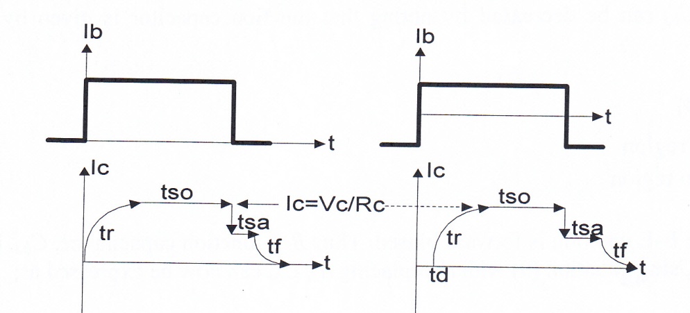
2.2. Digital Operation: In this mode input signal is sufficient to drive the transistor in to On/Off regions. Operation mode is usually referred to as Large Signal Model. The input signal is usually data 0 or 1 in the form of pulses. In this mode our concern is the switching speed of the transistor from Off to On region and vice versa. Basically there are two types of input pulses, unipolar and bipolar shown in Fig.4 with the transistor responses under each input type.
(a) (b)
Fig. 4 Transistor digital operation responses
(a) Uni-polar input pulse (b) bipolar input pulse
The responses are almost the same except for td in bipolar input. In addition bipolar input pushes transistor to turn off with sharper fall time, tf, thus steeper slope. But it requires bipolar power supply. We will consider only the uni-polar input. Fig 4 (a) shows four distinguished parts:
(1) Rise time, tr, due to all transients and capacitor charging times discussed in analog operation.
(2) Storage time, tso. Once the transistor enters On region, it becomes saturated and its collector current remains almost constant at Vc/Rc since during this time Vce ≈ 0, (0.1 – 0.3) depending on the type of the transistor, Ge or Si.
(3) Saturated time, tsa, required for the minority carrier to return to base.
(4) Fall time, tf. After removing the input Ic decrease to zero with a different time constant. Fall time is longer than the rise time, tr, due to returning the accumulated charges in the collector region.
The ON/Off times can be derived from either charge transport model or from Ebers – Moll equations. Using charge transport method, tr and tf are given by [4];
Carrier recombination time
β current gain, Ic/Ib
In addition to above, collector saturation time, ts is given by [2];
N/I normal/inverted mod
ω cutoff frequency
α current gain, Ic/Ie
Total transistor switching time will be the sum of all above delays time is:
T sw = tr + tf + ts (21)
Table 3 is a short summary of above delays for 2N3904 transistor [5].
Table 3 – Transistor switching times
| Type of Delay | Designation | Delay Time (ns) |
| Rise time | tr | 50 |
| Fall time | tf | 90 |
| Storage time | tso | 800 |
| Saturation time | tsa | 1 |
To decrease the switching time, we must increase cutoff frequencies by decreasing the storage capacitors especially the collector junction capacitor. A second method is to use Emitter Coupled Logic (ECL) shown in Fig. 5, [6]. This configuration is used both in analog and digital integrated circuits. In analog it cancels fluctuations in the power supply by providing high Common Mode Rejection Ratio (CMRR), and in digital it provide fast switching without either transistor entering On or Off region, operating in the active mode with shorter swinging amplitude.
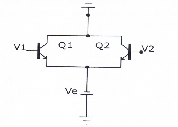
Fig. 5 Emitter coupled logic, (ECL)
3. Propagation Delay
This term refers to input- output relation as a whole in digital integrated circuits rather than the delay in individual component. Digital integrated circuits are made of several directly interconnected transistors in different configurations such as TTL, ECL, and CMOS – transmission delay between input and the output is referred to as propagation delay [7]. Overall delay is the sum of individual transistors delays as discussed in the previous sections. Thus, there is no need for developing new theories to evaluate propagation delay constant. However, this type of delay has a significant effect on data transmission. Fig. 6 shows a typical effect of this delay on the output of an And Gate. Note especially, if the delay is one pulse width as in (b), (note impossibility), the output, (A1. B1─ ) becomes zero! In such case, since the propagation delay time is specified in manufacturer specification, the only choice to improve the situation is to change the input pulse width to at least ten times larger than the delay time. Unfortunately this will also constrain the speed of data transmission, see problem 8.
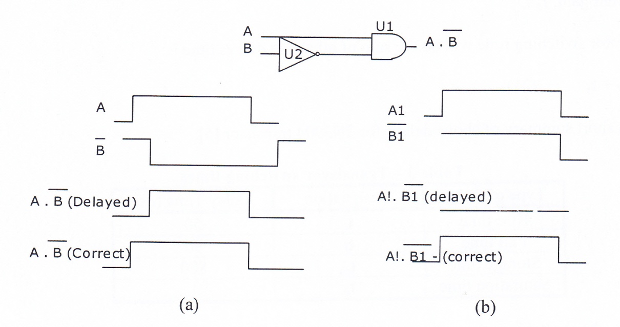
Fig. 6 – Effect of propagation delay
We conclude this section with the most popular digital integrated circuit configurations shown in Fig. 7 with their approximate delay times given in table 4, [8]. ECL configuration seems to be the fastest switch except for the losses associated with Rc and Re. This circuit can be converted to a losses Bi-CMOS technology configuration by replacing these resistors with active elements, such as MOSFETs [9]. Finally, CMOS configuration has the least power consumption as is used in the ROM, except the model is not suitable for switching due to large built in capacitor in the gate.
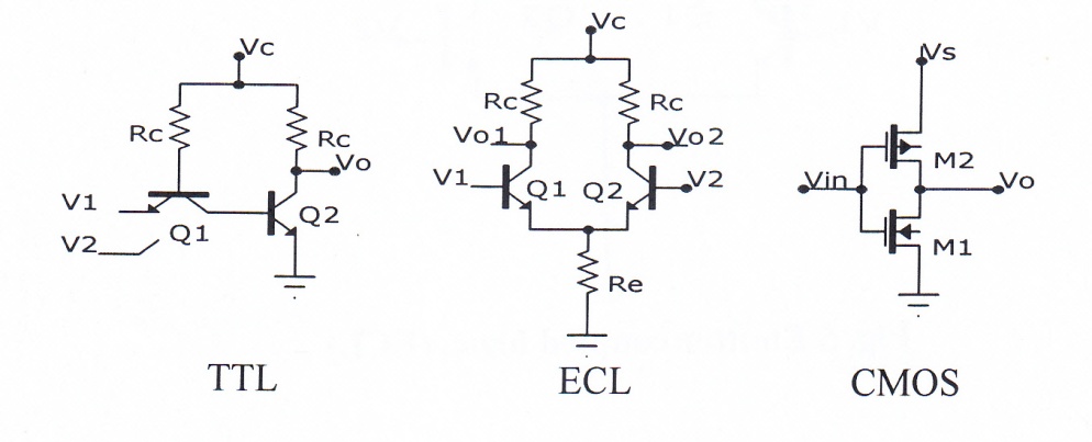
Fig. 7 – Most popular digital IC circuits
Table 4 – Typical characteristics of popular IC
| Configuration type | Power Consumption (mW) | Propagation Delay time (ns) |
| TTL | 10 | 10 |
| ECL | 25 | 2 |
| CMOs | 0.1 | 25 |
4. Slew Rate Effect
This term is usually referred to the slope of output voltage with respect to time as applied to intrinsic operational amplifier shown in Fig. 8.
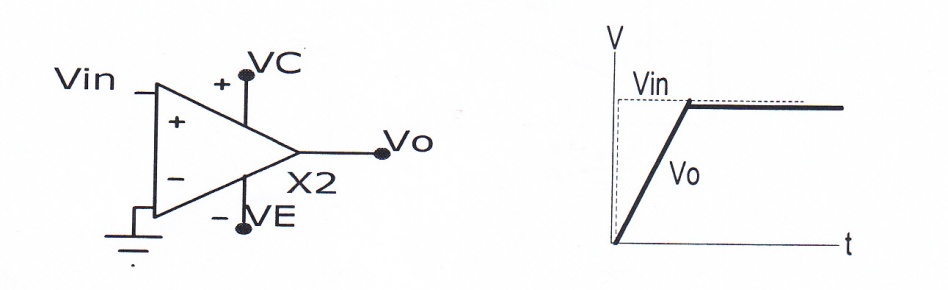
Fig. 8 – Ideal response of an Op/Amp to a step function
Delay shown is for ideal response. The actual response will depend on the loading of Op/Amp and it would look exponential charging capacitor in an RC circuit. In approximate form it is similar to rise time considered in the previous sections. It is due to transient and capacitor charging time effects. Since it is the intrinsic properties of the device, it can only be improved by careful device fabrication. Its typical values for different Op/Amp is cited in Table 5 for a reference [10]
Table 5 – Typical values of slew rate for popular Op/Amps
| Type | 741E | CA3140 | LH0042C |
| Slew rate V/µs | 0.7 | 9 | 3 |
5. Hysteresis Time Delay
This term refers to delay between input and output state in comparator circuits. Fig 9 is a schematic of a two level comparator used extensively in control processing. For this circuit the input applied at terminal 3, non-inverting terminal, is shown to be a sine wave of enough amplitude to cause the state of the output to change. Simulated input-output is shown in Fig. 10. The output is almost a square wave with a delay, i.e. when the input becomes zero; the output still maintains a small positive value as is evident from the blue line. This is called hysteresis effect, somewhat similar to ferromagnetism. In general output does not change state immediately from high to low. This delay has a significant effect in industrial control processing. With a careful design this delay can be controlled as explained below.
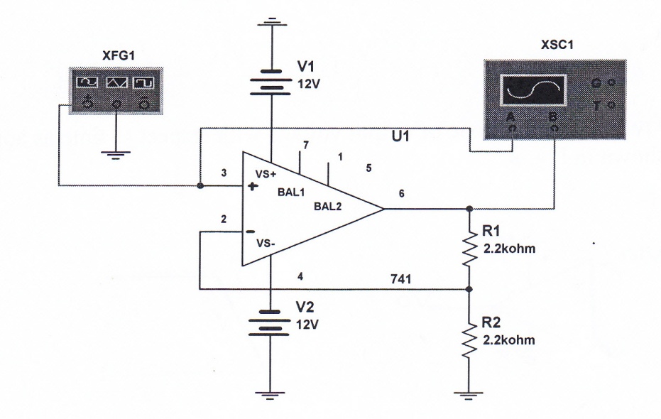
Fig. 9- Schematic of a two level comparator
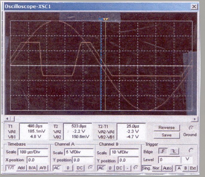
Fig.-10 Input-output wave-forms for two level comparator shown in Fig. 9.
Normalized hysteresis time, th is given by [11]
T period of sine wave input
V– negative square-wave output voltage(usually is given)
Vp peak voltage of applied sine wave
Using above figure with x-axis sensitivity of 100 µs/Div, the delay between input-output (blue- red vertical lines) is about 4µs. It is clear from the above equation that selection R1 and R2 play an important rule to reduce the hysteresis time, th. But unfortunately their selections also affect the noise margin. This is the parameter which enables comparator not to switch back and forth under small fluctuations, higher its value, the better the performance of comparator. Its normalized value is given by [11];
V+ is the high level output square wave voltages. This equation indicates that noise margin, n is in conflict with hysteresis time, decreasing th will also decrease n, causing comparator to mall function, unwanted switching back and forth. A plot of n and th are shown in figure 11. Since n is an increasing function but th is a decreasing function of R2, the intersection of these two curves establishes the proper choice for R1 and R2. Since there are four possible choices, consideration of power consumption can help to select the best values for R1, and R2.
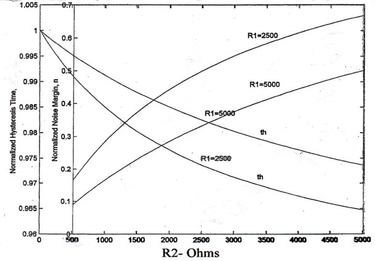
Fig.11 Optimal design of two – level comparator. The intersection of two curves establishes an optimal selection of R1 and R2 to obtain maximum n and minimum th.
This finishes our trial for Series 2. Our next series will be an exciting topic about Colors Secrets which has never been published before. Hope it will be ready by the time you finish this series.
Thank you for your interests
The Authors
References
[1] Shyh Wang, Solid State Electronics, McGraw-Hill Inc., 1966, pp. 136-140, L.C. 65-28136.
[2] S. M. Sze, Physics of Semiconductor Devices, Joyn Wiley & Sons, Inc. 1969, pp. 279-282, , 302- 309, ISBN 471 84290 7.
[3] Donald A. Neamen, Semiconductor Physics and Devices, Richard D. Irwin, Inc., 1992, pp. 417-419, ISBN 0-256-08405-X.
[4] Ben G. Streetmen, Solid State Electronic Devices, Prentice-Hall, Inc., Englewood Cliff, N.J., 1980, pp., 142 – 147, ISBN 0-13-822171-5.
[5] C. J. Savant, Jr., Martin S. Roden, Gordon L. Carpenter, Electronic Design,The Benjamin/Cummings Publishing Company, Inc., 1991, pp. A-86 – A-91, 690-692, ISBN 0- 8053-0285-9
[6] H. Javan, H. A. Kalhor, “ECL Receiver Stability,” IBM Project 3A, Contract No. KGN – Uo25 Electrical Eng. Dept., State Univ. of New York, New Paltz, New York, 12561, Feb. 1988.
[7] Herbert Taub, Donald Schilling, Digital Integrated Electronics, McGra-Hill, Inc., 1977, ISBN 0-07-062921-8.
[8] M. Morris Mano, Digital Design, Prentice-Hall, Inc., Englwood Cliffs, New Jersey 07632, 1984, pp. 60-68, ISBN 0-13-212325-8
[9] H. Javan, H. Chamas, “A lossless stable voltage sources for high speed applications,” in the First Industry/Academy Symposium on Research for Future Supersonic and Hypersonic Vehicles, TSI Press, Division of TSI Enterprises, Inc., 1994, vol. 1, pp537 – 542, ISBN 0- 9627451-8-9
[10] Donald A. Neaman, Electronic Circuit Analysis and Design, Richard D. Irwin, a Times Mirror Higher Education Group, Inc. company, 1996, p.824, ISBN 0-256-11919-8.
[11] H. Javan, “Industrial measurement,” in the Applied Instrumentations, ch. 4, pp.4-6- 4-8, Dept. of Eng. Tech., Univ of Memphis, TN 38152, to be published.
Problems
1. A piece of conductor is connected to a voltmeter as shown. Electrons are moving at random directions as shown with the thermal velocity given by equation (2), what will be the voltmeter reading? Why?
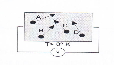
Fig 12 Problem No 1
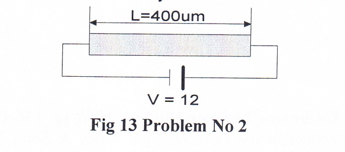
2. A piece of n-type GaAs which has a mobility µn = 8500 (cm2/V-sec) is connected to a 12 V DC voltage source as shown. Neglecting thermal velocity, determine electron drift velocity. Device can be used as an oscillator, called Gunn diode mistakenly.
3. A pulse voltage is applied to a RG/59 transmission line which is 500 meter long and has a dielectric constant, . How long will it take for the pulse to reach the end?
Fig 14 Problem No 3
4. In transistor analog operation, which parameter or the element limits the transistor H.F. response?
5. For the typical values given in table 2, determine H.F. limit of that transistor.
6. Determine the shortest input pulse width for the transistor given in table 3.
7. Refer to Fig. 6 and table 4. Using ECL configuration with 2 ns delay time, what must be data transmission rate for the input pulses?
8. Determine Vo for TTL and ECL circuit shown in Fig.7, with V1=Vc, and V2=0.
9. Using Table 5, how long will it take a 1Volt input to reach steady state using 741E Op/Amp?
10. Drive equation 22.
11. Noise margin is the difference between two reference voltages. For Fig. 9 they are given by:
Drive equation 23.
12. Using Fig. 11, determine the four possible values of, R1 R2, pair for optimum response. Which pair would be the best possible choice?